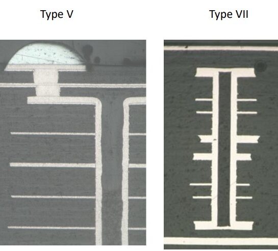
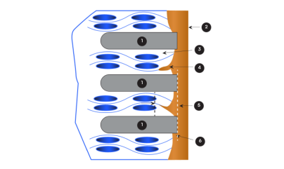
Both structures show buried vias but the left Type V is not capped with copper while the right has copper plated over the epoxy filled buried via. Please note the thicker overall copper on Type VII in comparison of type V. With the reduced copper we are able to achieve the following:
- Thinner base copper Type V allows for finer spacing.
- Type V has 20-25 less processing steps which can reduce cycle times from 1-3
days. - If Type VII is invoked missing cap plating is considered non-conforming.
- If Type VII is invoked a deep dimple greater than allowed per IPC-6012 table 3-11 would be considered non-conforming.
- If Type VII is invoked cap plating less than allowed per IPC-6012 table 3-11 would be considered non-conforming.
Type V does not have any of the last three requirements which makes compliance moreassured with the fewer process steps. The reduced base copper diminishes shorts and provides for higher yields.
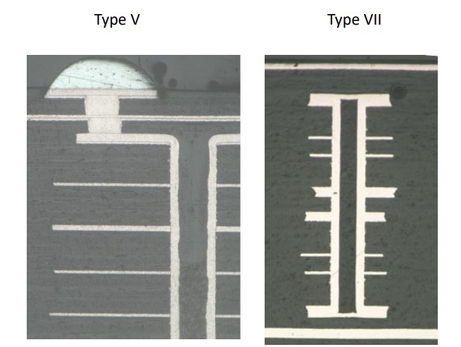
The definition and purpose of Type V:
This information can be found in IPC-4761 Section 5.5 and table 5-1. Section 5.5 “A via with material applied into the via targeting a full penetration and encapsulation of the hole. Both section 5.5 and Table 5-1 state that Type V is beneficial to “useful in sequential lamination process”. It states the same benefit for Type VII, but there is no explanation on what it is for either Type V or VII.
Here are the Type V benefits.
- Benefit 1 Lower Base Copper Allows for Smaller Conductor Space:
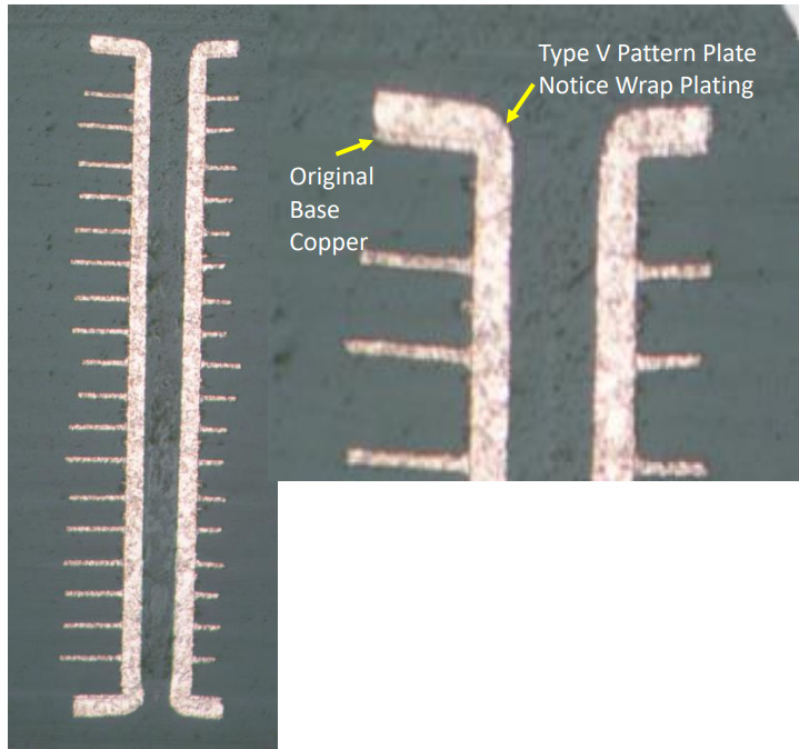
- Type V does not require wrap plating (if this is new to you and you have via in pad or callout epoxy fill please see IPC-6012 section 3.6.2.11.1). Standard wrap plating increases the base copper of outer layers drilled in the buried structure. The wrap plating thickness can vary in the process and increased space is needed for etching. Type V does not require this process so the base copper remains at the starting copper and allows for finer space with best yields. The pattern plate of the outer buried layers will naturally plate copper that wraps from the via onto the outer buried layers.
- Benefit 2 Less Process Steps Faster Cycle Time:
- Type V builds reduce between 20-25 PCB fabrication process steps. The Buried structure is laminated, drilled, hole prepped, Electroless, pattern plate, etched and epoxy filled. Please note the fill is after etching the outer layer pattern of the buried structure. This is followed by next lamination structure.
- Benefit 3 Most Important The Filled Via Holes After Etch Prevent Resin Loss in Vias.
- If the buried vias were not filled the resin in the prepreg from the next lamination cycle would be squeezed out of the woven glass and into the the open buried vias. This loss of resin could lead to a dangerous condition where the resin is “starved” out of the weave between the buried sub and next layer (typically the outer layer foil). The resin starvation could allow moister to soak into the outer dielectric which could have a delamination event during assembly or the application of HASL (Hot Air Solder Level). Type V filling prevents the resin loss and protects the finished PCB from the resin starvation condition.
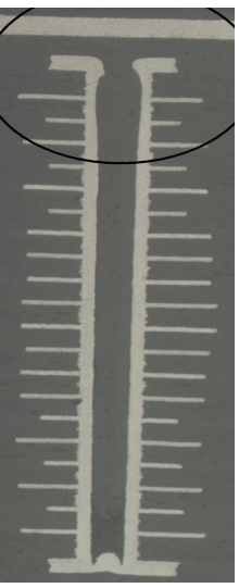
- Type V does not require Type VII requirements that are considered non-conforming. Example of a Type V via that meets the requirement.
The definition and purpose of Type VII:
As stated earlier, Type VII has the same benefits as Type 5. The definition of Type VII can be found in IPC-4761 section 5.7.
Additional Benefits:
- Via in Pad, but wait this a buried via structure that we are talking about. So there is no benefit when the via structure is buried.
- Via Stacking, DON’T DO THIS! A microvia on a type VII buried via will fail almost 100% of the time. STAGGER THE MICROVIA AWAY FROM THE TYPE VII
Requirements for Type VII that don’t benefit a buried via:
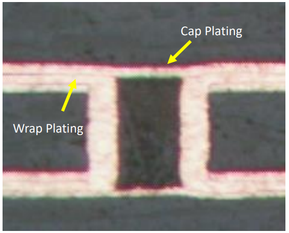
- Cap plating, since a buried via land is buried it’s a wasted requirement. However a source inspector will reject an order if the cap plating is missing and the buried via is specified as a Type VII or cap plated.
- Wrap plating which is required if it is Type VII, this is needed for reliability. When wrap plating is required we are targeting a thickness of 200 or 500 micro inches minimum, and a process target window of 400 micro inches. Needless to say this increases the difficulty and requires that the design has enough space for the added wrap copper on top of the base copper. After pattern plate the fabricator must etch thru the original base copper and added wrap plated copper. Adding to the complexity is the variation of wrap plating thickness. This can create variation in conductor height and width on outer buried via layers. If you are an RF or Signal Integrity Engineer you most likely won’t like this variation.
- Maximum allowed dimple is .003” for class 3 and .005” for class 2. Again, if a source inspector finds a dimple that exceeds these values, it would be considered a non-conforming condition. If type V or VII did have a dimple of .010” it could easily be filled with prepreg from the next lamination cycle without creating a resin “starvation” condition.
Type VII Buried Via (Simple Compliant)
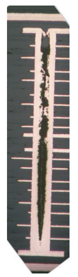
Type VII that are non-compliant but meet fit form and function, and if defined as Type V would have been acceptable.
Here is a condition where Type VII was required and a non-conformance condition occurred, but if Type V was allowed this condition would not have occurred.
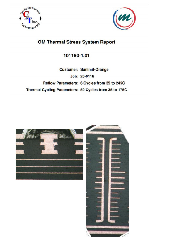
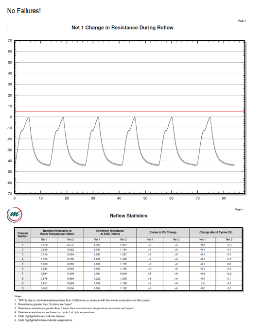
Here is the OM Test Results of A buried via job with Type V vias.
In Summary:
HDI Designs that have buried vias will benefit by specifying IPC-4761 Type V instead of Type VII.
- Reduced cycle times saving 1-3 days in PCB fabrication
- Lower conductor spacing. Typically .0005”- .001” lower.
- Higher fabrication yields translates to better on time delivery and at full quantity.
- Less non-conforming conditions and requests for compliance waivers.
- Consistent conductor thickness
There are few instances where the Engineer (consistent signal performance) , the Designer (smaller features), and Fabricator (shorter cycle time & higher yields) all benefit from the same practice. Thank you for listening to a fabricators input!
More articles
What is New in IPC-6012 Revision F?
IPC recently released an update to IPC-6012. Revision F covers qualification and performance specifications for ...
10 Causes of Lamination Voids and Ways Designers Can Prevent Them
One of the challenges in printed circuit board (PCB) manufacturing is the occurrence of lamination ...
How to Thoughtfully Design Embedded Cavities into a PCB
The increasing demand for compact, high-performance and reliable electronic devices requires novel solutions to address ...