Icon about-block-ico-1 Icon about-block-ico-2 Icon about-block-ico-3 Icon about-block-ico-4 Icon announcement-close Icon arrow-left Icon arrow-right Icon arrow-sm Icon asterisk Icon banner-transparent-vector Icon btn-callback-ico Icon careers-item-location Icon careers-item-time Icon careers-item-type Icon careers-mail-ico Icon careers-phone-ico Icon careers-search-ico Icon careers-single-hero-vector Icon careers-single-more-vector Icon careers-vector Icon check Icon close Icon dfm-image-left-vector Icon dfm-image-right-vector Icon document Icon download-popup-vector Icon dropdown Icon envelope Icon facebook Icon faq-banner-bg Icon faq-title-ico-active Icon faq-title-ico Icon featured-links-block-bg Icon figure-1 Icon figure-10 Icon figure-11 Icon figure-12 Icon figure-13 Icon figure-14 Icon figure-15 Icon figure-2 Icon figure-3 Icon figure-4 Icon figure-5 Icon figure-6 Icon figure-7 Icon figure-8 Icon figure-9 Icon file-upload Icon form-sidebar-back Icon form-step-done Icon gmap-marker-group-icon Icon gmap-marker-icon Icon header-profile-ico Icon instagram Icon link Icon linkedin Icon loader Icon mail Icon phone Icon play-yt Icon play Icon post-nav-arr-left Icon quote-banner-vector Icon quote-block-aside-vector Icon quote-contact-phone-ico Icon quote-contact-position-ico Icon sidebar-location Icon sidebar-phone Icon technology-banner-nav-left-vector Icon technology-banner-nav-right-vector Icon twitter Icon webinar-item-date-vector Icon whitepaper-img-ico-left Icon whitepaper-img-ico-right Icon whitepapers-listing-banner-ico Icon whitepapers-single-aside-vector Icon youtube Icon yt-play-button
header-top-card Your connection to advanced PCB manufacturing
Download a Brochure
Advanced PCB Technology

Semiconductor ATE

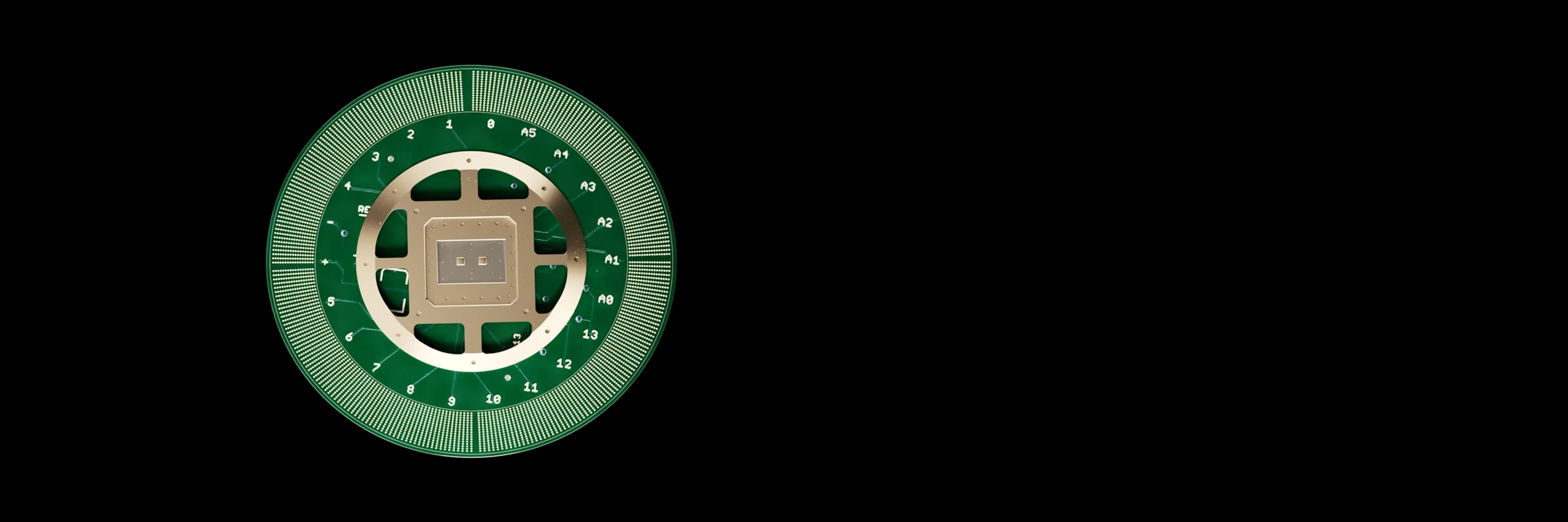
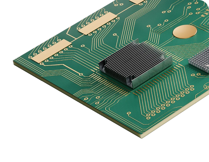
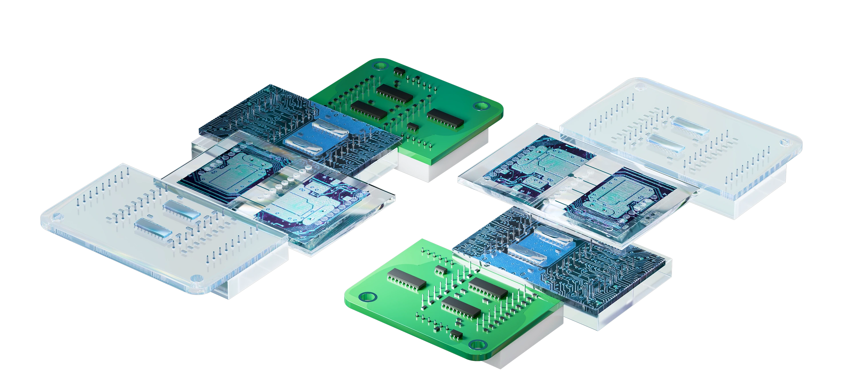
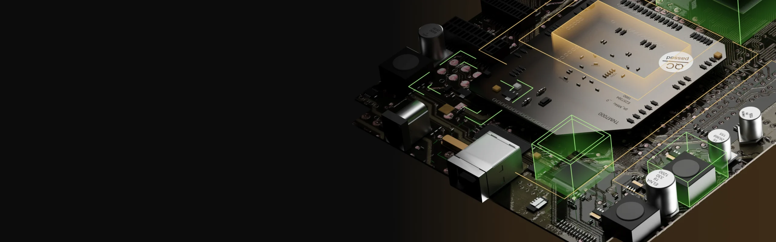
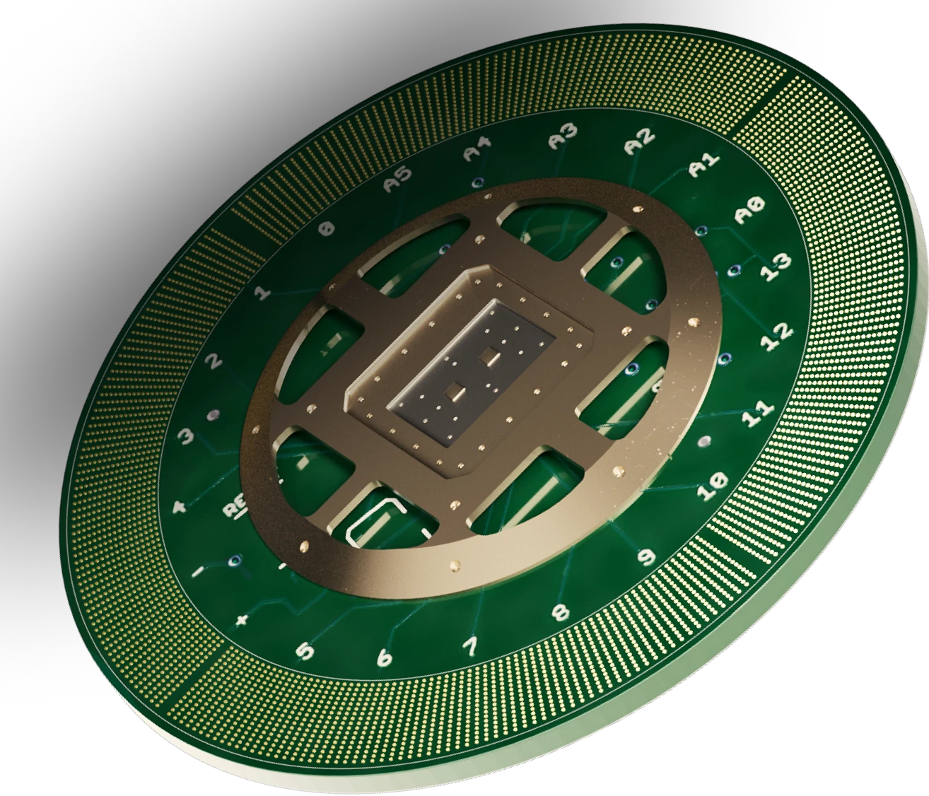
Automated Test Equipment (ATE) boards are used for testing highly complex semiconductor chips. ATE board designs are typically highly complex with an emphasis on high performance. The boards have an extremely high layer count (40 to 60+).

Certifications & Memberships

  • IMAGE OF ICP LOGO
  • PCBAA Proud Member Badge
  • Image of USPAE logo
ATE PCB Capabilities

What ATE boards demand

  • 40–60+ Layer Counts

    ATE designs require extremely high layer counts for the routing density and signal isolation needed to test sophisticated semiconductor chips.

  • Controlled Impedance

    High-speed digital design requires precise impedance control throughout — a prerequisite for accurately exercising advanced semiconductor chips.

  • Precision Via Structures

    Microvias, blind vias, and buried vias — each requiring tight dimensional control and consistent plating quality.

  • High-Frequency Materials

    Signal integrity at high frequencies depends on advanced material selection — the laminate choice directly affects performance and reliability.

Specialized Services

What Summit builds for ATE

Summit’s ATE offering goes beyond raw layer count. These are the specific board types, finishes, and services we provide for semiconductor test programs.
  • 01

    Reference design test boards

    Validated for ATE environments

  • 02

    High aspect ratio ATE boards

    60+ layer specialty builds

  • 03

    Bondable gold finish

    Wire-bond ready surfaces

  • 04

    Tight tolerance drilling

    Precision to ±0.025mm

  • 05

    Copper balancing

    Controlled impedance layers

  • 06

    Quick turnaround services

    Expedited without compromise

Why Summit

The complexity your ATE program demands

Summit has extensive, first-hand experience manufacturing the large, multi-layer specialty boards that semiconductor ATE demands. Our customers can efficiently test portions of their semiconductor designs in less time, with improved reliability.
These boards are not standard PCBs. The layer counts, via structures, and performance requirements exist at the outer edge of what PCB manufacturing can achieve. Summit is built for exactly that.

Solutions
FAQ

Frequently asked questions

  • Vias are critical to achieving high interconnect density, especially in HDI designs. Summit uses microvias, blind and buried vias, and via-in-pad structures to route complex circuits within tight spaces. These features reduce signal path length, improve electrical performance, and allow for higher component density without increasing layer count.

  • The annular ring is the copper pad area surrounding a drilled hole, and maintaining precise dimensions is essential for electrical and mechanical reliability. Summit’s laser and mechanical drilling processes, combined with tight registration control, ensure annular ring integrity in accordance with IPC-6012 Class 3 requirements, even on microvia and fine-pitch designs.

  • HDI PCBs support higher signal speeds by shortening trace lengths, reducing parasitic inductance, and enabling controlled impedance routing. This is critical for high-frequency and high-speed digital designs used in computing, telecommunications, and advanced electronics.

  • Building an HDI PCB often requires multiple sequential lamination cycles, laser drilling, copper filling, planarization, and precise imaging for fine-line features. Each step must be tightly controlled to maintain dimensional accuracy and electrical performance, especially for mission-critical applications.

  • We follow lean manufacturing principles, minimize scrap through precise process control, and use IPC standards to reduce rework and waste. By optimizing yields on complex builds, Summit supports both operational efficiency and environmental responsibility.

The most demanding ATE programs start here

Talk to our engineering team about your ATE PCB
requirements. We’re ready to review your design and tell
you exactly what we can build.

MSIRobot