
header-top-card Your connection to advanced PCB manufacturing
Download a Brochure
Engineering support

Design for Manufacturing (DFM)

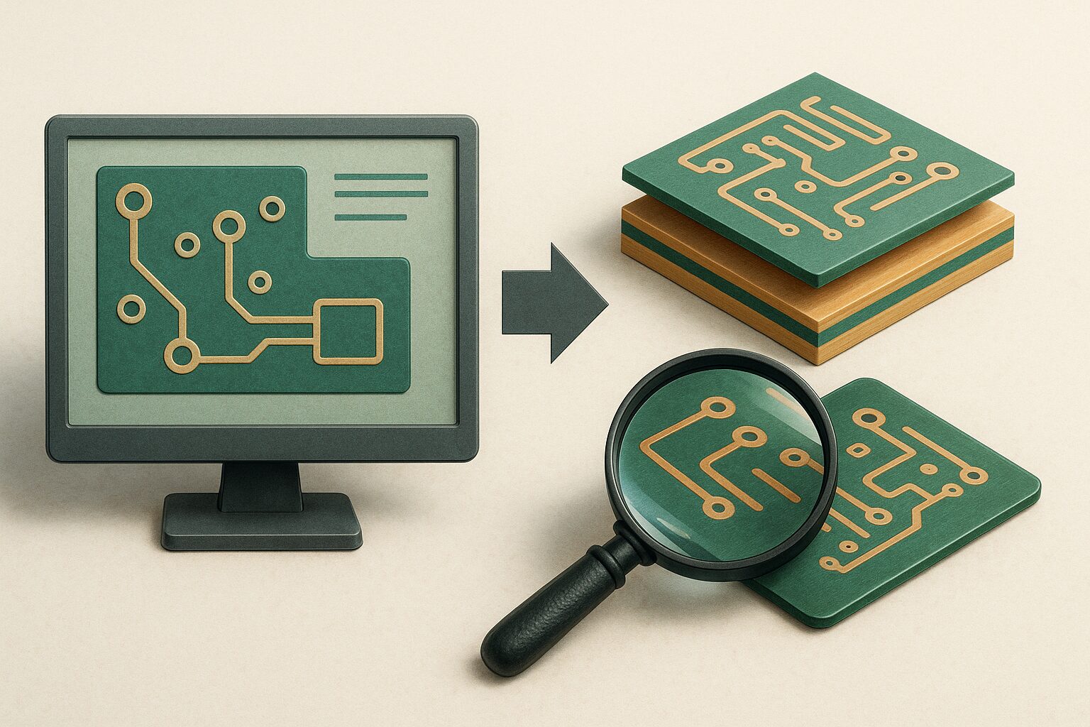
Summit’s Design for Manufacturability (DFM) services identify manufacturability issues early in the design process, helping to reduce the risk of design revisions and production delays

  • Reports in 1–5 days
  • Manufactured in the United States
DFM Reports

Two levels of analysis. One goal: first-pass yield.

Choose the depth of analysis that fits your schedule and design stage — from a rapid automated check to a full tooling deep-dive.

  • Automated Report 1–2 Business Days

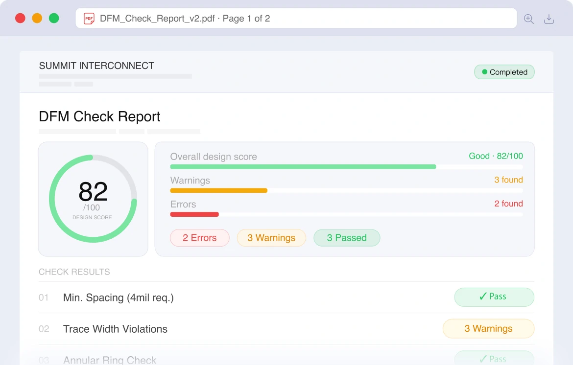
    DFM Check

    An automated analysis of your Gerber files that surfaces common design rule violations before fabrication begins. Fast, reliable, and a critical first pass for any PCB design.
    • Minimum spacing violations
    • Minimum trace width violations
    • Annular ring integrity checks
    • Netlist consistency verification
    Get Started
  • Detailed Analysis 3–5 Business Days

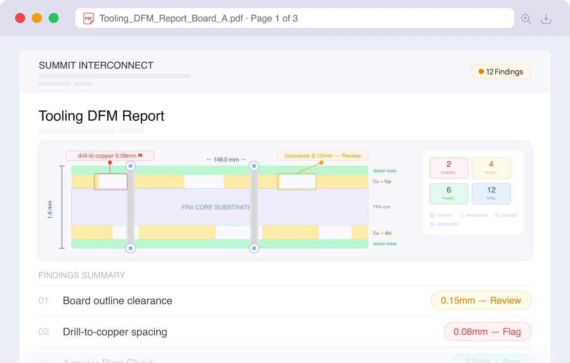
    Tooling DFM Report

    A comprehensive engineering review with visuals and findings across your full board specification. Ideal for complex or high-reliability designs where first-pass yield is critical.
    • Board outline & clearance review
    • Drill diameter & pad size analysis
    • Drill-to-copper & trace-to-trace spacing
    • Conductor width & board thickness specs
    Get Started
DFM Review

Ready for a DFM Review?
Start your Quote.

Our engineers are ready to review your Gerbers, stackup
documents, and drawings. Get an automated DFM Check in as little as 1–2 business days.

From quote request to actionable feedback

A straightforward process designed to get your design reviewed and back to you — fast.

  • Submit Design Files

    Submit your Gerbers, stackup documents, and drawings via our secure portal to begin your quote.

  • Select Report Type

    Choose a DFM Check for a rapid automated review, or a Tooling
    Report for a full engineering deep-dive.

  • Engineering Review

    Our FAE team analyzes your design against Summit’s manufacturing capabilities and industry standards.

  • Receive & Iterate

    Get your report with actionable findings. Our team is available to
    walk through results and support design revisions.

Design for Manufacture Services (DFM)

Download our DFM brochure to learn how Summit Interconnect’s Design for Manufacturability process helps identify potential manufacturing challenges early, improving yield and accelerating time to production.

News
FAQ

Frequently asked questions

Quick answers to questions we hear most often

  • Vias are critical to achieving high interconnect density, especially in HDI designs. Summit uses microvias, blind and buried vias, and via-in-pad structures to route complex circuits within tight spaces. These features reduce signal path length, improve electrical performance, and allow for higher component density without increasing layer count.
  • The annular ring is the copper pad area surrounding a drilled hole, and maintaining precise dimensions is essential for electrical and mechanical reliability. Summit’s laser and mechanical drilling processes, combined with tight registration control, ensure annular ring integrity in accordance with IPC-6012 Class 3 requirements, even on microvia and fine-pitch designs.

  • HDI PCBs support higher signal speeds by shortening trace lengths, reducing parasitic inductance, and enabling controlled impedance routing. This is critical for high-frequency and high-speed digital designs used in computing, telecommunications, and advanced electronics.

  • Building an HDI PCB often requires multiple sequential lamination cycles, laser drilling, copper filling, planarization, and precise imaging for fine-line features. Each step must be tightly controlled to maintain dimensional accuracy and electrical performance, especially for mission-critical applications.

  • We follow lean manufacturing principles, minimize scrap through precise process control, and use IPC standards to reduce rework and waste. By optimizing yields on complex builds, Summit supports both operational efficiency and environmental responsibility.

Ready to Start your Next
PCB Project?

Fast, flexible, and reliable PCB solutions for your next project.

MSIRobot