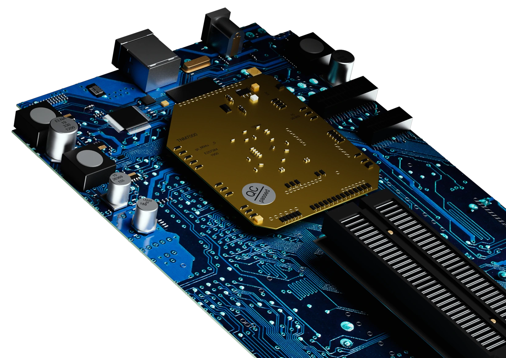
Each board is built to applicable industry standards and customer requirements, with processes designed to deliver repeatable quality from prototype through production.
From Design File to Finished Board: Precision PCB Production

Production
What PCB Production Actually Involves
PCB production transforms your design data into a finished, electrically tested circuit board. The process moves through carefully controlled stages, including intelligent analysis, automation data extraction, imaging, chemical processing, drilling, plating, surface finishing, and testing. Because the accuracy of each stage affects the next, quality checks are built throughout the process rather than reserved for final inspection.
Production Stages
Our PCB production process
-
01 – 06
Engineering and prep
[01]-
Design data is reviewed and converted into a production plan. The engineering team performs manufacturability checks, defines the stackup and materials, plans panelization, verifies impedance requirements where applicable, and creates the manufacturing instructions, or traveler, before the job reaches the production floor.
-
Base laminate materials are issued according to the approved stackup, with material certifications and lot information recorded to maintain traceability throughout the manufacturing process. The laminate is cleaned and coated with a light-sensitive material called photoresist, while prepreg materials are prepared for lamination as required.
-
-
02 – 06
Inner layers
[02]-
Direct imaging (DI) exposes the circuit pattern onto the photoresist-coated laminate. The photoresist is developed, unwanted copper is etched away, and the remaining resist is stripped to reveal the finished inner-layer circuit pattern.
-
Inner layers undergo Automated Optical Inspection (AOI) to identify potential defects and verify alignment with the design data. The copper surfaces are then treated to promote adhesion, and the inner layers, prepreg, and copper foil are stacked and pressed together under controlled heat and pressure to form a multilayer panel.
-
-
03 – 06
Drilling and hole prep
[03]-
Panel edges are trimmed as needed, and X-ray drill optimization is performed to verify layer alignment and achieve best-in-class registration. Through-holes and vias are then drilled using controlled drilling programs.
-
When specified by the design, laser drilling is used to create microvias and other precision features. Drilled features are then treated using chemical or plasma processes, as required, to remove resin smear or laser residue and expose clean internal copper. Etchback may also be performed when needed so subsequent copper plating can form reliable interconnections.
-
A thin, conductive layer of copper is chemically deposited onto the hole walls, preparing them for subsequent electrolytic copper plating.
-
-
04 – 06
Outer layers
[04]-
Photoresist is applied to the outer copper surfaces, and DI transfers the outer-layer circuit pattern. The resist is then developed to expose the areas that require additional copper plating.
-
Copper is electroplated to the required thickness, followed by a temporary tin coating that protects the circuit pattern during etching. The remaining photoresist is stripped, unwanted copper is etched away, and the tin is removed to reveal the finished outer-layer circuitry.
-
-
05 – 06
Finishing
[05]-
A protective coating (solder mask) is applied over the circuitry, shielding everything except the points that need to be soldered.
-
A specified surface finish, such as ENIG, ENEPIG, or lead-free or tin-lead HASL, is applied to exposed copper to protect against oxidation and maintain solderability.
-
Reference markings (still often called “silkscreen”) are printed onto the board to guide assembly.
-
-
06 – 06
Test and ship
[06]-
Each board is electrically tested against the design data to identify opens and shorts and verify circuit continuity before final inspection.
-
Individual boards and test coupons are routed from the production panel. Boards are inspected for dimensional accuracy and workmanship, and coupon cross-sections are evaluated as required to verify plating, layer alignment, and other construction requirements.
-
Finished boards are packaged to prevent damage and contamination, then shipped with the required documentation and lot traceability.
-
Solutions
Board Types & Solutions We Work With


Materials
The laminates, prepregs, copper foils, and flexible substrates used to form the physical and electrical structure of a PCB. Materials are selected based on design requirements such as operating frequency, signal loss, thermal performance, flexibility, reliability, and manufacturability. Common options include FR-4, low-loss and RF laminates, flexible polyimide materials, and materials designed for thermal management.
Selected based on
-

FR-4
-
Low-loss and RF laminates
-
Flexible polyimide
-
Thermal management materials


For Engineers
Technical glossary
-
The copper pad area surrounding a drilled hole. Maintaining the required annular ring dimensions supports electrical and mechanical reliability.
-
Camera-based inspection that compares a fabricated circuit layer with the design data to identify potential opens, shorts, and imaging or etching defects.
-
A fixtureless electrical test method that uses independently controlled probes to contact designated test points on a PCB. It verifies electrical continuity and isolation to identify potential opens and shorts and is well suited for prototypes, low-to-medium production volumes, and complex designs.
-
A via connecting an outer layer to one or more inner layers but not passing through the entire board.
-
A via connecting two or more inner layers only, fully hidden within the finished board.
-
A design and manufacturing requirement that keeps a transmission line’s impedance within a specified tolerance to support signal integrity in high-speed and RF applications.
-
The process sequence that develops the imaged photoresist, etches unwanted copper, and removes the remaining resist to reveal the circuit pattern.
-
Chemical or plasma treatment that removes resin smear from drilled hole walls so copper plating can bond directly to exposed internal copper.
-
-
A review of design data against manufacturing capabilities and process rules to identify potential issues before fabrication, reducing the risk of revisions and production delays.
-
A thin conductive copper layer deposited by chemical reaction (no electrical current) to seed hole walls for subsequent electrolytic plating.
-
Copper deposition driven by electrical current, used to build trace, pad, and via-barrel copper to final thickness.
-
Common PCB surface finishes: electroless nickel immersion gold (ENIG), hot air solder leveling (HASL), and electroless nickel electroless palladium immersion gold (ENEPIG). These finishes protect exposed copper and maintain solderability.
-
The master instruction document that follows a job through every production stage, specifying stack-up, materials, and process parameters.
-
An electrical test method using movable probes rather than a dedicated fixture, typically used for prototype and low-volume boards.
-
PCB construction that uses features such as microvias, blind and buried vias, fine-line circuitry, and sequential build-up layers to achieve greater interconnect density in a smaller footprint.
-
Industry-published requirements and acceptance criteria used to guide PCB design, fabrication, inspection, and performance.
-
A patterning method that transfers digital circuit data directly onto photoresist using a controlled laser or LED light source, eliminating the need for traditional phototools.
-
The process of bonding inner-layer cores, prepreg, and copper foil into a single multilayer structure under heat and pressure.
-
A small laser-drilled via used in HDI designs, typically connecting adjacent layers. Microvias may be arranged in staggered to structures for higher interconnect density.
-
An outer-layer process that electroplates copper onto exposed circuit features and hole walls. A temporary metal resist protects the plated pattern while unwanted background copper is etched away.
-
Partially cured fiberglass-reinforced epoxy resin sheet used to bond layers together during lamination.
-
A drilled and copper-plated hole that provides electrical connection through the full thickness of the board.
-
A protective polymer coating applied over copper circuitry, leaving only solderable pads exposed.
-
Contact us
We’re available to answer any questions
-

Email Us
info@summitinterconnect.com -
Call Us
+1 (877) 264-0343


Follow Summit on LinkedIn, Facebook and Twitter and keep up with news and insights!