One of the challenges in printed circuit board (PCB) manufacturing is the occurrence of lamination voids, which can have a significant impact on the performance and reliability of the final PCB. In this blog post, we will explore lamination voids, what causes them, and how to mitigate their effects.
What Are Lamination Voids?
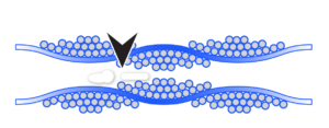
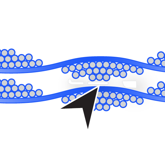
Lamination voids are areas of incomplete bonding between the layers of a multilayer PCB. These voids are essentially pockets of gases from thermal polymerization caused by the absence of epoxy resin within the PCB stackup. They can vary in size and shape, and their presence can lead to several issues, including reduced thermal conductivity, decreased mechanical strength, and impaired electrical performance.
Causes of Lamination Voids
Understanding the root causes of these voids is essential for preventing their occurrence. Causes of delamination include:
- Mismatched CTE (Coefficient of Thermal Expansion): One of the primary culprits behind lamination delamination is the mismatch in between different glass styles that has different thicknesses varying CTE ppm/C and due to lacking resin/glass encapsulation used in the PCB. An attribute that causes cohesive separation after thermal exposure is the resin backbone enthalpy along with moisture uptake. This leads to stress on the plated through-holes.
- Environmental and Machine Variations: The profile of lamination can vary depending on environmental conditions and machine parameters. It’s essential to set the profile correctly before initiating the lamination process to minimize void formation.
- Inaccurate Drill Values: Using incorrect drill values can lead to voids as they may disrupt deposition coverage during plating cycles.
- Uneven Copper Distribution: When copper is not distributed uniformly within the design of the circuitry, it can lead to resin recesses. To mitigate this, sufficient copper thieving (the unwanted areas of the circuitry) should be added to balance the copper distribution, thereby reducing void formation.
- Trapped Gases: Temperature control is critical during the curing of the resin used in lamination. Incorrect temperature profiles can lead to incomplete encapsulation and void formation.
- Insufficient Pressure: Insufficient pressure during the lamination process prevents the layers from bonding correctly, resulting in gaps that lead to voids.
- Inadequate Temperature Control: Temperature control is critical during the curing of the resin used in lamination. Incorrect temperature profiles can lead to incomplete bonding and void formation.
- Contaminants: The presence of contaminants like FOD, moisture, or impurities on the surfaces of the resin or copper foils can interfere with the lamination process and contribute to void formation.
- Poor Material Quality: The use of low-quality materials, including substrates and prepregs, can increase the likelihood of voids. Such materials may have inconsistent resin content or reinforcement, making them more susceptible to void formation.
Avoiding Lamination Voids
Lamination voids can have a detrimental impact on the overall performance and reliability of a PCB. Voids reduce the thermal conductivity of the PCB, leading to poor heat dissipation. The presence of voids can compromise the mechanical strength of the PCB, resulting in warping, cracking, or even outright failure. Finally, voids can disrupt signal integrity and impedance matching, leading to electrical problems. This can result in signal loss, increased electromagnetic interference (EMI), and decreased overall functionality. Paying careful attention to stackups and the distribution of copper on the board can help minimize the occurrence of lamination voids.
The Role of Stackup Design
Proper stackup design is the cornerstone of preventing PCB lamination voids. A well-considered stackup design involves selecting the right materials and arranging them in a way that minimizes the chances of void formation. Here are some key considerations for effective stackup design:
- Material Selection: Choosing the right laminate material and prepreg style is crucial. Materials with low moisture absorption and good thermal properties are preferred to minimize the risk of voids. Additionally, using high-quality prepregs can help prevent voids.
- Copper-to-Prepreg Ratio: The ratio of copper to prepreg is essential for promoting proper adhesion between layers. Gas is a mass that requires to be evacuated to then allow resin/glass to compress onto it avoiding lamination void. But keep in mind you must know the window for resin to flow with minimal resistance. This is for example Rate of Rise required to reach <= 1,000 pascal. The lower viscosity, the purer the resin.
The Role of Copper Distribution
In addition to stackup design, copper distribution plays a critical role in preventing PCB lamination voids. Here are the key considerations for effective copper distribution:
- Uneven Pressure Distribution: A significant difference in copper thickness between the various layers can result in uneven pressure distribution during lamination. When there’s a substantial imbalance, it can lead to voids forming in regions with less copper, as the pressure might not be distributed uniformly.
- Use Copper Fill Techniques: Copper fill techniques, such as adding copper pours or ground planes, can help maintain uniform copper distribution while enhancing thermal performance.
In conclusion, PCB lamination voids can be a significant concern, potentially compromising the functionality and reliability of electronic devices. However, by focusing on stackup design and copper distribution, designers and manufacturers can significantly reduce the risk of void formation. Collaboration between designers and PCB manufacturers is key to ensuring that the chosen materials, stackup configuration, and copper distribution are optimized for each specific project, resulting in robust and reliable PCBs for a wide range of applications.
More articles

From Layout to Fab: Gerry Partida’s Top DFM Guidelines for PCB Designers
Originally published July 10, 2025 by Judy Warner at The Electronics Eecosystem When it comes to ...

RF & Microwave PCB Design: Navigating High-Frequency Complexity with Precision
RF and microwave PCBs aren’t just signal carriers—they’re performance enablers. In the GHz realm, every ...
Understanding Controlled Impedance in High-Frequency PCB Design
Controlled impedance is crucial in printed circuit board (PCB) designs that operate at high frequencies ...