IPC recently released an update to IPC-6012. Revision F covers qualification and performance specifications for rigid PCBs. Below are some of the important changes included in this revision and how they can impact PCB design and manufacturing.
As a rule, IPC documents do not provide background as to why the changes are made or the cause and effects that the changes bring. In this resource document, Summit shares the changes and the impact on the PCBs to help the industry to better understand the benefits of the newest revision and insight how and why these changes are needed.
______________________________________________________________________________________________________________________________
Revision F New Section 1.4.3
Back Drill Depth
The new section 1.4.3 was added to allow for clarity on where a back drill measurement is evaluated when back drill depth is specified. This was necessary since the back drill starting point could be considered as it is specified in section 1.4.2, or it could have been considered at the starting foil or the total copper thickness. With the new section the measurement is clear and does not take the surface copper into consideration for validating the depth.
It is Summit’s recommendation that the back drill specified using the attributes of figure 1-1 and all of the notes 1-6.
- Design considerations when a design has back drills in plated holes.
- Specify the side to back drill and the must not cut (MNC) layer.
- Review the design distance between the back drill diameter and conductors adjacent to the back drills path.
- Create a separate drill program for each back drill type/span.
- Create a drill chart and specify back drill, diameter with count.
- Specify if plated hole to be back drilled is to be epoxy filled or not filled.
- Specify if back drill is to be epoxy filled after back drilling.
- Specify Stub length allowance.
- Clearly specify if the back drill is to be plated over and attached to an external ground plane. Also include if the PCB fabricator must modify the data to achieve a finished copper ground fill over the back drill.
- Also note that some imperfections of copper over the epoxy filled back drill is allowed per IPC-6012 sections 3.3.1, 3.3.9, 3.6.2.19 and 3.6.2.20
______________________________________________________________________________________________________________________________
Revision F Section 3.6.2.14.1
Plated Internal Layers
This section is new in the base document, but was actually part of IPC-6012 AM1 (Amendment 1), which was published in March of 2022. It is important to understand that the section is actually not a change but a clarification for the requirements for an internal plated layer. Before the amendment it was not clear if the internal plated layer should be treated by the rules for external layers and follow the table “Thickness of External Conductor of the Finished Printed Board after Plating” (Table was Table 3-15 in IPC-6012 rev E, and is now Table 3-18 revision F) or if the evaluation follow the table for “Internal Layer Copper Thickness after Processing” (Revision E table 3-14 and now in revision F table 3-17). It was unclear which rule was to be used, creating confusion, and possible rejections of parts if the external rule was to be used instead of the internal thickness rule.
This was for many years a heavy and difficult debate within the IPC committee until the rule was finally clarified with section 3.6.2.14.1.
Section 3.6.2.14.1 Plated Internal Layers – When internal layers are plated the minimum total thickness (copper foil plus copper plating) shall be in accordance with Table 3-17 (This is the internal layer copper thickness table). The minimum copper foil as specified shall be used prior to plate. When the overall finished conductor is specified in weight rather than thickness, the minim conductor thickness after plating shall be the minimum thickness after processing from Table 3-17 for that particular copper weight. The initial copper foil used prior to plate may be reduced to a maximum of 50% of the minimum thickness after processing from table 3-17. Absence of copper foil at the knee of the hole due to processing shall not be for rejection so long as the minimum wrap plating onto foil is present. All other plating requirements (e.g., wrap or cap plating) shall be met and can be included in the final measurement for total thickness.
The new section clarifies that the internal plated layer will follow the lower total copper requirement found in table 3-17 plus wrap plating and cap plating if it is required. For the PCB designer/Engineer that allowed for this rule there is no change. For the engineers that were relying on the Thickness of External conductors Table 3-18, there is a concern that the conductor could be much thinner.
For example, if a fabrication drawing calls out ½ ounce on an internal plated layer that has a blind via terminating on the layer, we would follow table 3-17 minimum thickness 11.4µm [.000449”] plus minimum wrap plating 5µm [0.000197] which would equal 16.4µm [0.000646”].
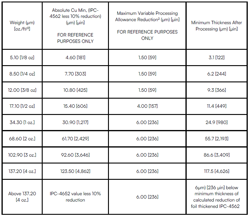
For those that previously used the external layer rule they would expect the total thickness for class 3 to be 38.4µm [0.001512].
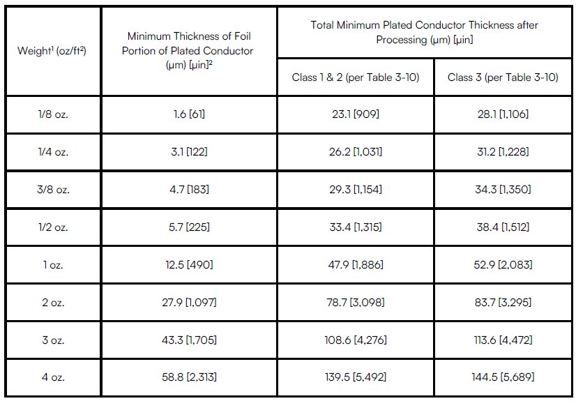
The difference is 22µm [0.000866”] which is significant.
Additionally, this section points out to another rule that must be considered by the design when the drawing specifies the layer copper thickness as a finished thickness.
When the overall finished conductor is specified in weight rather than thickness, the minim conductor thickness after plating shall be the minimum thickness after processing from Table 3-17 for that particular copper weight.
When the print specifies finished thickness by weight, Table 3-17 is in effect which is the lower total conductor height. Typically, the outer layer has final plated thru holes which will add about an ounce of copper to the outer layer surface which will equal to or exceed the requirements of the external Table 3-18. However, if there are no final plated thru holes and the print stated finished copper weight instead of starting, there is no need to add to the starting foil beyond the requirements of wrap and cap plating per IPC-6012. The designer should take into consideration whenever the copper foil is specified as finished in ounces. Please note, that copper is considered starting thickness unless the document states finished.
Benefits of section 3.6.2.14.1
- There is now clarity on acceptance for a plated internal layer. There have been cases where the fabricator applied the current rule but had the boards rejected when the end user applied the conductor thickness for an external layer.
- With the allowance of a thinner conductor thickness for a plated layer, fabricators can plan stack ups with thinner dielectrics and avoid delamination or laminate voids. As the copper thickness increases there is a greater chance of glass stop or resin starvation between internal plated layers.
- Thinner total copper will lower conductor variation which allows for more consistent signal performance.
- Lowers overall PCB thickness with lower conductor thickness and the reduction of prepreg between plated internal layers.
- Opens up design envelope. Allows for greater range of impedance conductors.
Considerations
- Designers should calculate the minimum copper thickness per the Internal copper thickness per table 3-17.
- Use finished conductor thickness by actual thickness value and not in ounces.
- Take into consideration older designs that could result in lower plated internal layer thickness. Fabricators could start to target the now “clarified” acceptance criteria.
______________________________________________________________________________________________________________________________
Section 3.6.2.6.2 Copper Penetration.
New definition for evaluation of etchback.
Brief explanation of Etch Back.
Etchback refers to the controlled removal of the dielectric material around the plated hole during the manufacturing process. It is believed that the process is crucial for achieving proper adhesion of the plating to the inner walls of the hole. The evaluation involves assessing the depth and uniformity of the etchback to guarantee that the plating material adheres securely and uniformly to the substrate. Proper etchback is essential for minimizing signal loss, ensuring good electrical performance, and promoting the overall reliability of the PCB. Precise evaluation techniques, such as cross-sectional analysis and optical inspection, are employed to verify that the etchback meets the specified requirements, ultimately contributing to the functionality and longevity of electronic devices.
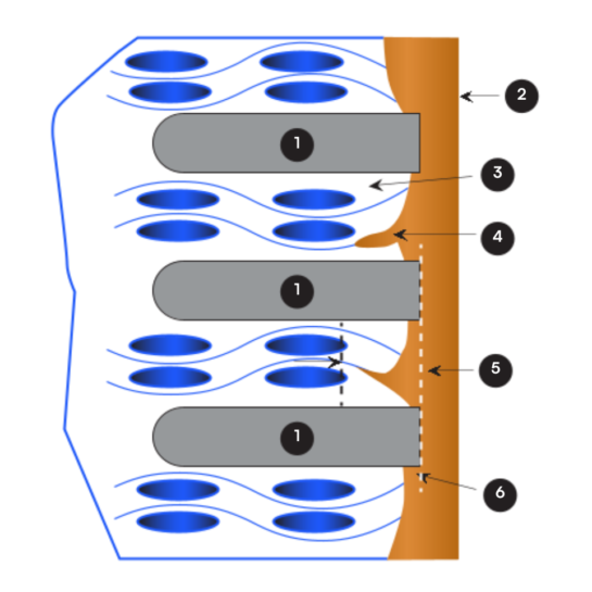
Etchback of a drilled hole is a condition required by the procurement documentation. Etch Back processing can be challenging for all of us that have had to plan, fabricate, or evaluate the etch back condition. There are limits to achieving etch back conditions and in the past the definition of how to evaluate etch back has been hard to convey and evaluate.
In earlier IPC-6012 revisions we have used images of an etched back hole and shown where the measurement begins, which is where the drilled pad is furthest in the hole after etch back, and the other end is. The other end is based on what was defined as “dielectric removal”, which is the result of wicking, random drill tears, or drill gouging and hole cleaning. With the old definition it is difficult to determine where the laminate material is no longer fractured away from the drilling process or from the hole processing. This is where the new definition Copper Penetration comes to the rescue.
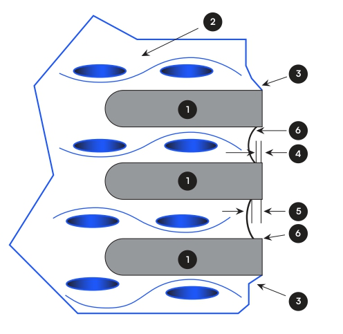
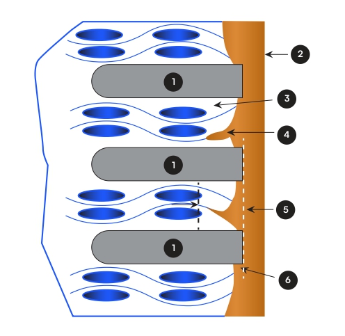
The evaluation for etch back is now defined as “Total Copper Penetration”. Essentially the measurement allowance is the same as IPC-6012 rev E, except now the measurement is from the drilled edge of the internal layer foil to as far back as the copper plating has penetrated. Table 3-8 is used to determine the maximum allowed copper penetration by class. IPC-6012 ref F has simplified the evaluation by eliminating the complicated definitions of what is removal in a cross section evaluation. The copper penetration allowance is the combined value of maximum etch allowance plus the maximum wicking based on Table 3-8. Example if a print state Etch Back 5µm-38µm[0.0002”-0.0015”] and table 3-8 Class 3 allowance states 80µm[0.00315”] then the maximum copper penetration allowance is max etch back 38µm[0.0015” + maximum wicking 80µm[0.00315] = maximum 118µm[0.0046”] Now etch back evaluation is simply to measure the copper penetration and confirming that the furthest penetration does not exceed 118µm[0.0046”] .
| Copper Penetration (see Figure 3-18) | Total copper penetration not to exceed the sum of both the 125µm [4,921 µin] maximum wicking allowance plus maximum etchback or smear removal allowance | Total copper penetration not to exceed the sum of both the 100µm [3,937 µin] maximum wicking allowance plus maximum etchback or smear removal allowance | Total copper penetration not to exceed the sum of both the 80µm [3,150 µin] maximum wicking allowance plus maximum etchback or smear removal allowance |
How does the new rule help? With the new clear definition, a fabricator that manages and controls etch back to the lower allowed value gains allowances for wicking that may occur during the drilling of a plated hole. Not all materials are equal, some materials, especially polyimide, show greater wicking than other materials. By managing the etchback to the minimum of 5µm[0.0002”] when a maximum allowed for etch back is 80µm[0.00315”], the finished product would allow more laminate removal, since the evaluation is total copper penetration. This new definition provides better clarity on how to evaluate, and has not actually changed the finished condition of the plated hole that was defined in IPC-6012 rev E.
Considerations:
- Training of Lab technicians to evaluate total copper penetration and not etch back and wicking as standalone evaluations.
- Training of source inspectors to understand that lab reports will only measure copper penetration and no longer as total removal.
- IPC-6012 revision F Space Addendum wicking evaluation, now under consideration, potentially will no longer have a stand alone wicking violation. Stay tuned to further developments in the Space Addendum. I will update if and when the modification has been accepted.
______________________________________________________________________________________________________________________________
Section 3.3.10 Printed Board Cavities
IPC-6012 Revision F finally introduces new rules specifically addressing the incorporation of cavities within PCB designs. The new rules reflect the dynamic nature of electronics manufacturing and the growing demand for innovative solutions in various industries. By establishing new rules and refining existing requirements, IPC-6012 Revision F strives to set a new standard for the design and manufacturing processes, offering engineers and manufacturers clearer guidelines to navigate the complexities associated with incorporating cavities into modern PCBs.
In this new section you will find that 3 types have been defined:
- Type 1 No Metallization on cavity floor or wall(s).
- Type 2 Metallization on either one or more walls, or floor, but not both.
- Type 3 metallization on cavity floor and adjoining wall(s) with continuous plating.
Cavities shall meet the dimensional requirements of the design. It is important that standard dimensional tolerances for a profile of the PCB is used for a cavity X and Y dimension. It is also important to keep in mind that the same CNC system that routs the profile of a PCB is used to make a cavity opening. A depth tolerance must also be stated. It is recommended to allow for a depth tolerance of +/-0.005”. Depths should be based on outer layer staring points and not a particular layer or dielectric.
Type 1 is simply a milled pocket in a PCB that allows for clearance of components to be placed upside down (dead bug) while having leads that can still be soldered to the outer layer surface.
Conditions of a Type 1 cavity
- The cavity floor shall be visually uniform in appearance.
- Exposure of disrupted fibers shall be in accordance with IPC-6012 section 3.3.2.6. (yes the woven glass will be disrupted if we are milling into the laminate. This should be expected.)
- When pre-cut prepreg/bonding materials are used in a cavity a non-laminated gap due to material misalignment may occur. This is allowed from the cavity wall up to 50% of the distance to the nearest conductor away from the cavity wall or 0.010” whichever one is less.
Type 2 would typically be a cavity that will allow for a wire bond land or placement of a component in a cavity to a desired internal layer. In this scenario the side walls of the cavity would be non-plated as a finished condition. Type 2 allows for components to directly connect to a desired internal layer. This application can provide better signal integrity performance. When using this method there are limits and concerns regarding soldering and solder mask applications. Solder mask materials are not engineered to be applied to a sub lamination internal layer and then to be subjected to a lamination cycle. Finished solder mask adhesion and appearance may not meet the requirements of IPC-6012 3.7 Solder Mask Requirements. It is highly advisable to review your design with Summit if a type 2 design required.
Conditions for a Type 2 cavity:
- For cavity conductor features continuous in plane, protruding from the cavity wall, adhesive flow is allowed up to 0.75mm [0.0295”] onto the conductor features. This is the same value found in IPC-6018.
- For lands on the cavity floor that encroach 0.75mm [0.0295”] from the cavity wall, adhesive allowance shall be AABUS. This implies if this condition is found a review with a fabricator should take place. Otherwise, there is a possibility of resin flowing onto a solderable land.
- When pre-cut prepreg/bonding materials are used in a cavity a non-laminated gap due to material misalignment may occur. This allowed from the cavity wall up to 50% of the distance to the nearest conductor away from the cavity wall or 0.010” whichever one is less.
For type 2 and 3 cavities the following applies:
- Unless otherwise defined in the procurement documentation, pristine areas of conductor features on the floor of a cavity require solderable or wire bondable finishes, excluding the allowable adhesive flow area, is defined by the central 60% area of the feature outline (round, rectangle, square, etc.) and shall meet the workmanship requirements of 3.5.4.
- For type 2 cavities with plated walls and type 3 cavities, when visually examined in accordance with 3.3, plating and coating voids in the cavity walls shall not exceed that allowed by Table 3-6 (new in rev F). Each sidewall of plated cavities shall be evaluated individually. Multiple voids on the same sidewall shall not have a combined area exceeding the area percentages.
| Material | Class 1 | Class 2 | Class 3 |
|---|---|---|---|
| Copper | Up to 20% of the sidewall area can be voided. Voids shall not exceed 60% of either the length or depth of the sidewall. | Up to 10% of the sidewall area can be voided. Voids shall not exceed 40% of either the length or depth of the sidewall. | Up to 5% of the sidewall area can be voided. Voids shall not exceed 20% of either the length or depth of the sidewall. |
| Finish Coating* | Up to 20% of the sidewall area can be voided. Voids shall not exceed 60% of either the length or depth of the sidewall. | Up to 10% of the sidewall area can be voided. Voids shall not exceed 40% of either the length or depth of the sidewall. | Up to 5% of the sidewall area can be voided. Voids shall not exceed 20% of either the length or depth of the sidewall. |
* Note 1. Edges of intentional edge plating interruptions are not required to have final finish coatings (i.e., exposed copper allowed in these areas).
Design Considerations
- Drills next to cavities should follow rules for features on the edge of the PCB. Conductors should be 0.020” from the edge cavity edges. This is a common oversite in Cavity designs, features are placed too close to the edge and can cause a rejection for accepting the design for manufacturing. Having features too close to the edge can create unfavorable manufacturing yields. If your design has features close to the cavity edge it is best to review the design with Summit.
- Plated holes outside the cavity wall should be pulled back at least 0.030” from the cavity edge.
- Vias in the cavity flow should be plated, filled, and cap plated per IPC-4761 Type VII. These vias should not be open.
- Solder mask on cavity floors should be avoided, and if required may not meet finished solder mask requirements per section 3.7.
- Review surface finish requirements in cavity area with Summit.
- Cavity PCB yields can be impacted by the processing requirements.
- Turn times are longer for cavity PCBs and increase by the number of required cavities.
______________________________________________________________________________________________________________________________
Section 3.3.1 Edge Plating New Paragraph Added to Edges
New Paragraph:
When printed board edge plating is specified, the following shall apply:
Plating separation from internal anchors (see IPC-2228) along the plated edge is not allowed. Edge wall pull-away from the dielectric shall be acceptable provided all the dimensional requirements are met. Plating voids shall not exceed 3 locations within the perimeter of the plated edge and not be greater than 1.27 mm [0.050in] in any length. Nodules on plated edges shall be acceptable as long as they are not loose and do not violate the overall printed board dimensions. Exposed bare copper is allowed on edges of breakaway (processing) tabs after final profile routing. Metallic burrs at breakaway (processing) tabs are acceptable as long as they are not loose and/or do not affect fit and function. Plated edge wrap onto the surface shall be within the dimensional limits of 3.5.1.
IPC-6012 revision F and IPC-2228, which was released in Oct 2022, are the first IPC documents that address design and performance requirements for edge plated printed boards. IPC-2228 is an excellent guideline for designing an edge plated PCB. See IPC-2228 Section 6.4.
Here are a few edge plated design considerations:
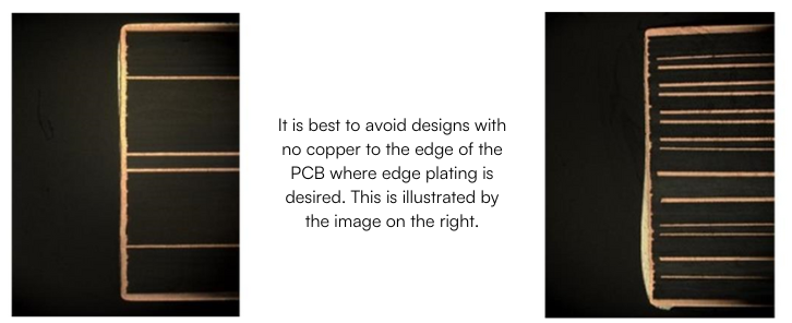
- Wrap the copper. Copper plating on the edge of the PCB has very low peel strength. The high outer layer copper peel strength in a typical PCB is accomplished by coatings on the copper foil that promote adhesion between prepreg and the copper foil. A plated edge of the PCB is milled/routed by a router bit which leaves a smooth almost polished surface. This smooth surface has electroless copper deposited and does not have any benefit of an adhesion promoter. Wrapping the copper onto the outer layer surface will take advantage of the copper foil adhesion promoters that anchor the top and bottom of the edge plating. Edge plating can easily peel off the edge if the design has no wrap plating. It is recommended to wrap the top and bottom surface by .63mm[0.025”]. While this value seems large keep in mind that the profile most PCBs is .254mm[0.010], and for the worst case scenario it is beneficial for adequate wrapping of the copper onto the outer layer copper.
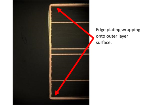
- Extend copper to the edge of the PCB. Edge plating adhesion can be improved by extending copper beyond the edge of the PCB. The copper will be exposed by the milling/routing operation where edge plating is desired. The exposed copper will act as anchors for the edge plating which reduces “pull away.”
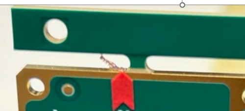
Here is an exaggerated example of edge plating pull away.
- Edge plating should only connect to the ground net. It is very important to pull back copper for all other layers where edge plating is desired.
- Pull back all copper on all layers for non-plated edges, include the allowed demarcation tolerance.
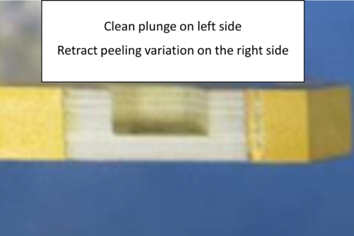
- Allow for generous demarcation tolerance between edge plated and non-plated edge of the PCB. The demarcation is created by a milling/ routing operation and as the spindle is rotating (at high speeds) the plunge of the bit is fairly clean but the pull out can pull the low peel strength edge plating. These pulls can range from target location to up to 0.020” additional pull and loss of edge plating of the side of the PCB. See example below.
Considerations:
- Understand the rules for edge plating in IPC-2228 (Released Oct 2022) section 6.4.
- Allow for generous dimensional tolerances for the demarcation of the transition from non-plated to plated edge. The demarcation/transition is not exact. Accuracy of demarcation of +/-0.025” would be beneficial.
- Only extend copper for ground layers pull back all other layers.
- For non-plated edges pull back copper on all layers.
- Document on your procurement documentation that copper to the edge of the PCB is by design.
- Edge plating should be used for ground shielding and not as a conductor. Position accuracy and length accuracy is not practical.
______________________________________________________________________________________________________________________________
Table 1-2 Default Requirements
IPC-6012 default Table 1-2 is an often overlooked or unknown table that exists in all of the performance specifications IPC-6012, IPC-6013 and IPC-6018. These tables provide fabricator allowances to process and fabricate a PCB when the procurement documentation does not state the requirements for the following attributes.
New changes in table 1-2 are highlighted in YELLOW.
As a rule, IPC documents do not provide background as to why the changes are made or the cause and effects that the changes bring. Summit, with the help of this blog series, has been sharing the changes and the impact on the PCBs to help the industry to better understand the benefits of the newest revision and insight how and why these changes are needed.
Here is a short summary of the three changes and how and why they have come about.
Surface finish ENIG.
With the common usage of ENIG over Tin/Lead finishes, fabricators use less and less Tin/Lead finishes and it is not uncommon to find ENIG processing inhouse, with Tin/Lead processing subcontracted to an outside service. Additionally, running a Hot Air Solder Leveling HASL can incur over $25k per month in electrical power costs. ENIG surface finish also provides a uniform coplanar surface that is beneficial to assembling SMT components. The new change has a “cut in date”. All initial releases of a drawing will still follow the old rule of Tin/Lead only when a surface finish not specified. Starting with initial release dates on the drawing as of October 1, 2023 when a finish is not specified the fabricator may use ENIG, Tin/lead, or Pb-Free solder coating (another change to table 1-2). This will allow the fabricator to make the most cost effective, and efficient finish between the 3 finishes listed in Table 1-2.
Dielectric Separation
The minimum dielectric has new lower default value of 65um [2,560u”]. This new change will allow fabricators to make dielectric thickness decisions for HDI/Laser drilled dielectrics without requesting thickness lower than the previous revisions minimum allowance of 90um[3,543u”]. Most microvia dielectrics use nominal thicknesses between 75um-100um[3,000u”-4,000u”]. This nominal range would either violate the old minimum or would always be on the edge of being noncompliant. This new change will prevent jobs being placed on hold in the Front End Engineering process, or deviation requests on finished product to allow for a lower minimum dielectric.
Solder Coated Pb-free
Fabricators will be able to use Pb-free solder coating if the surface finish is not specified. This will reduce the need to have HASL systems that run both Tin/Lead and PB-free systems in the same factory.
Considerations:
- The default surface finish will now have multiple options. If these options need to be controlled, it will be necessary to have the surface finish specified in the incoming procurement documentation.
- Dielectric minimums will be lower and withstanding voltages should be reviewed in high voltage designs.
- Allowance of Pb-free solder coating may introduce solder incompatibilities.
______________________________________________________________________________________________________________________________
Section 3.6.2.6.1 Evidence of Etchback
Evidence of Etchback (When Specified) When only evidence of etchback (i.e. visual evidence of lateral removal of resin and/or glass fibers) is specified by procurement documentation, no more than two layers per hole shall show zero etchback. All other layers shall have etchback greater than zero.
This is a new section that has been added to section 3.6.2.6, and it is very important to understand and apply correctly.
When the procurement documentation allows for evidence of etchback there is an allowance for no evidence of etchback on no more than 2 layers. This new rule helps for high aspect ratio holes at greater than 10:1 and have small diameter drilled holes, typically .25mm [0.010”] or less. For these small diameter holes it is difficult to achieve evidence of etchback in the center of the hole and it does impact yields. The new rule allows for 2 layers in the middle of a plated hole to have no evidence of etchback. This change will be highly beneficial for improving fabrication yields.
Reflow and thermal shock testing of plated holes via IPC-TM-650 methods 2.6.27 and 2.6.7.2 with etchback, evidence of etchback, or no etchback have demonstrated the ability to pass reflow and thermal shocks. These results support this allowance in this revision of IPC-6012 rev F.
When applying the rule there must be some internal layers that show evidence, but in the event of stackups with more than 4 layers this rule is applied when evidence of etchback is specified.
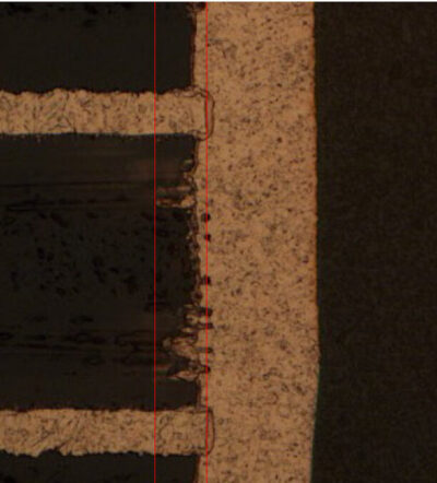
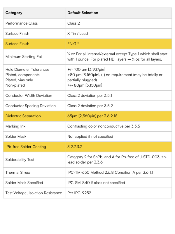
Below is an example of a 12:1 aspect ratio with 1 layer with no evidence of etchback. Rejected in IPC-6012 rev E and now acceptable in IPC-6012 rev F. Please consider that source inspection training will be needed for correct evaluation of this section.
______________________________________________________________________________________________________________________________
Section 3.6.2.18.1 Minimum Dielectric Spacing
If the minimum dielectric is unspecified, a new minimum dielectric spacing will go into effect for drawings with an initial release date after December 31, 2023. The new rule going into effect 1/1/2024 will have a minimum of 65um [0.00256”] when the minimum dielectric is not specified. For designs released before the cutoff date the old minimum dielectric rule will remain for those designs. The minimum dielectric before the cutoff date was 90um [0.003543”] and will remain so because of the cutoff date 12/31/2023.
So why the change? Microvias
Typical microvia stack ups will target a dielectric between 60um-100um [0.0025” to 0.004”] to manage the microvia aspect ratio. If a HDI design does not specify minimum dielectric for the expected range, it is easy for the finished PCB to measure below the previously allowed minimum thickness of 90um [0.003543”]. To prevent delays and rejecting parts that need a lower minimum, fabricators need to present a request for a new minimum allowed dielectric to ship finished product. New designs will no longer have this potential delay.
After 12/31/2023, new initial released HDI designs can be planned and released to manufacturing without requesting a new minimum dielectric. This new rule will reduce time consuming delays to request an AABUS (as agreed between user and supplier) for finished product or a new design that is the planning stage.
Considerations:
- This rule only applies if the initial release is after 12/31/2023.
- All designs with initial release before 1/1/2024 will follow the old rule.
- Both thickness and cut in dates are in IPC-6012 rev F section 3.6.2.18.1
- This does not apply to revision changes.
- Source inspection training will be needed for correct evaluation of this section.
______________________________________________________________________________________________________________________________
IPC-6012 revision E section 3.6.2.11.3 – Dimples and Protrusions
Microvia dimples and protrusions are no longer AABUS. IPC-6012 revision E section 3.6.2.11.3 second paragraph started with “Requirements for protrusions (bumps) or depressions (dimples) in blind copper filled microvias shall be AABUS.
Revision F now has a new table 3-14 (3-14 is no longer the table for Internal Layer Foil Thickness after Processing) Table 3-14 is now titled “Depression and Protrusion in Copper Filled Microvias.”
| Designed Hole Diameter | greater than 0.15 mm [0.006 in] | less than or equal to 0.15 mm [0.006 in] |
|---|---|---|
| Filled Via Depression (Dimple) - Maximum | 50 µm [1,969 µin] | 25 µm [984 µin] |
| Filled Via Protrusion (Bump) - Maximum | 25 µm [984 µin] | 25 µm [984 µin] |
Note 1: Applies to microvias in lands intended to be soldered at assembly.
What is interesting with this addition is that the table does not use classes but is broken down by laser via diameters. Depression/dimple allowance is 25µm/0.000984” for a microvia that is less than or equal to 0.15mm/0.006”, and if larger than the depression/dimple maximum is 50µm/0.001969.”
For protrusions/bumps the number remains the same for any microvia diameter that is plated shut with a maximum protrusions/bumps of 25µm/0.000984.”
It is important to note that the Table 3-14 only applies to microvias in lands intended to be soldered at assembly. In all other microvia location that are not intended to be soldered at assembly the protrusion and dimples are not rejectable when all other conditions have been met.
If more stringent finished conditions are required, please document your AABUS (As Agreed Between User and Supplier) on your procurement documentation. For best practice please add your requirement on the fabrication drawing.
Please stay tuned for other changes in IPC-6012 rev F from Summit Interconnect.
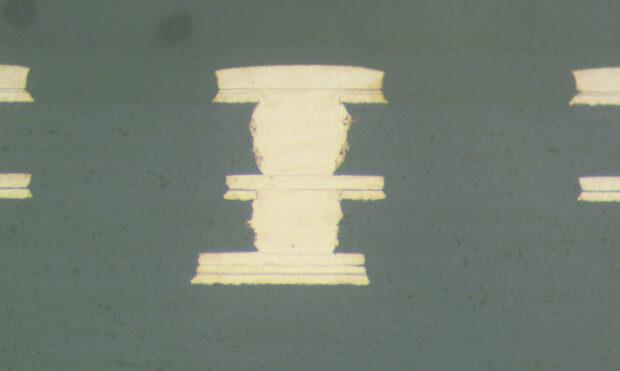
Here is a picture of a microvia with a dimple.
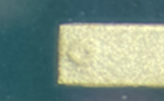
And one with a protrusion.
For any further questions about changes in IPC-6012 Revision F or for technical questions, Summit Interconnect is here to assist. Email our field applications engineering team at fae@summitinterconnect.com.
More articles

Understanding Controlled Impedance in High-Frequency PCB Design
Controlled impedance is crucial in printed circuit board (PCB) designs that operate at high frequencies ...

Sustainability in PCB Design: Insights from Summit Interconnect at IPC APEX EXPO 2025
At IPC APEX EXPO 2025, Gerry Partida, VP of Technology at Summit Interconnect, sat down ...

The Key to First-pass Success in PCB Design
In the dynamic world of PCB manufacturing, achieving first-pass success hinges on more than just ...