The increasing demand for compact, high-performance and reliable electronic devices requires novel solutions to address the challenges of thermal management, higher component density and signal integrity. One such solution is the incorporation of embedded cavities into printed circuit board (PCB) designs.
If a designer wants to include an embedded cavity in their PCB, then certain guidelines must be followed based on fabrication capabilities and industry standards. There are important design considerations regarding embedded PCB cavities to keep in mind, as well as a close eye on documentation preparation and formatting to ensure that design intent is fully understood by a manufacturer.
What are cavities in a PCB?
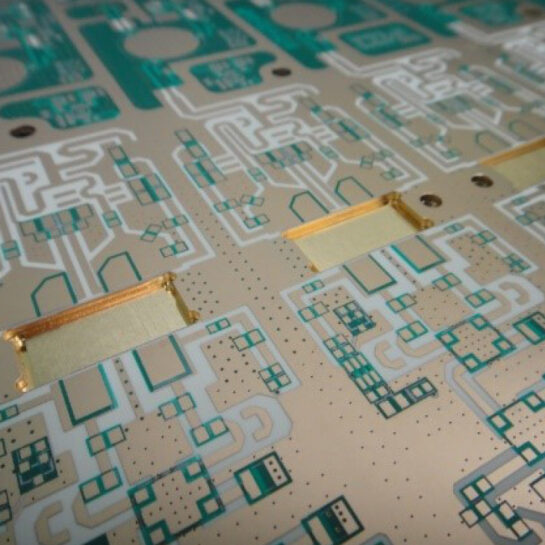
Embedded cavities in a PCB are recessed areas or pockets deliberately designed and fabricated on the outer or inner layers of a PCB. Cavities are fabricated by removing material from dielectric layers through controlled-depth CNC routing. These regions can be plated on the walls or floors, or they can expose etched copper in the floor or layers. When exposed copper is present in a cavity, these cavities may be used to mount components or be used as wirebond lands.
Types of embedded cavities
There are four main types of embedded cavities:
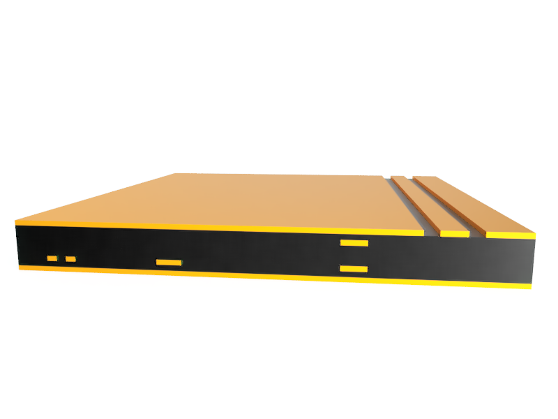
- Cavity that has no metallization on the floor or walls. This is the newly defined Type 1 Cavity in IPC-6012 Rev F due to be released later in 2023.
- Edge-plated cavities, where the edge of the cavity region includes copper plating.
- Embedded component cavities, where etched copper is exposed on the floor or ceiling of the cavity so that surface mount device (SMD) components can be mounted or for wirebonding. When there is metallization in either the floor or wall but not both, the cavity is considered a Type 2 cavity.
- Solid copper cavity, where a cavity floor and wall is completely metalized and filled with solid copper; this is considered a Type 3 cavity.
- Cavities can be placed between layers or within a surface layer; inset cavities are fabricated into a surface layer and can include exposed pads where SMD components can be mounted.
How embedded cavities are used
There are various uses of cavities that enable new approaches to designs, particularly when low profile assemblies are needed, or thermal management is a challenge. There are several design ideas for using embedded cavities in a PCB.
Embedded components
Although not the most common application of embedded cavities, components that would have been mounted on the surface layer could be placed internally in a cavity and mounted directly to exposed copper. The exposed copper allows direct connection to a signal trace, large power rail or ground pour on an internal layer, so vias are not needed to make the connection. This could be useful for high-speed designs or high-frequency designs. For example, coupling capacitors on differential lines could be placed on an internal layer with this strategy, thus eliminating vias.
For convenience of placement and routing, it is possible to size a cavity such that multiple components could fit into a single cavity. This could be done for mounting, for example, an array of decoupling or bypass capacitors for a large digital processor. This strategy eliminates two vias per capacitor, which reduces total inductance in the power delivery network (PDN) and expands the low-impedance range of PDN operation up to higher frequencies. Both factors are desirable in digital designs.
Inset components
This follows the same idea as in embedded components, but the inset places the components just below a surface layer. This allows the component to remain exposed to the environment while being mounted on an internal layer. Inset components decrease the total height profile of the board but remove some routing area on an internal layer. Additional routing space could be recovered by adding a layer to the stackup, but this increases costs. Although costs increase, a thin profile may be desirable for certain products, and this can outweigh the additional time and fee associated with cavity processing.
Thermal conductor or thermal insulator
The cavity fill material can be used to engineer heat flow throughout a device. While this is most commonly embedded copper being used as a heat sink – or thermal conductor – these cavities could also be filled with air to act as a thermal insulator. One should note that air-filled cavities may introduce mechanical strength challenges, as well as potentially enable moisture ingress and contamination. If the application requires high reliability, these aspects should be investigated in environmental testing at the device’s intended operating temperature, pressure and relative humidity.
In the case of copper coining as a heat sink, the cavity needs to be placed near the component being targeted for heat sinking. This could be easy in power systems, but it could be difficult for processors with high I/O count in digital designs. In the former type of design, this allows a power system to have much lower profile than would be the case with a large heat sink attached on the surface layer.
IPC design guidance
There are two main standards that designers should examine to better understand embedded cavity fabrication in PCBs: IPC-2228 and IPC-6012F. The IPC-2228 standard provides design guidance for high-speed or RF PCBs; this document acts as an extension to the existing IPC-2221 standards for high-speed or high-frequency products that may be built on advanced material systems.
Within the IPC-6012F standard, there are three definitions specifying different types of acceptable cavities in a rigid PCB:
- Type 1: A cavity with no metallization on the walls or floors
- Type 2: A cavity with some metallization on either the walls or floors
- Type 3: A cavity with metallization on both the walls and floors
Type 2 cavities would typically be used for component mounting by allowing etched copper to remain present on the upper or lower copper layers. Type 3 cavities are the type that would be used to form an embedded heat sink.
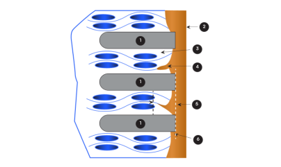
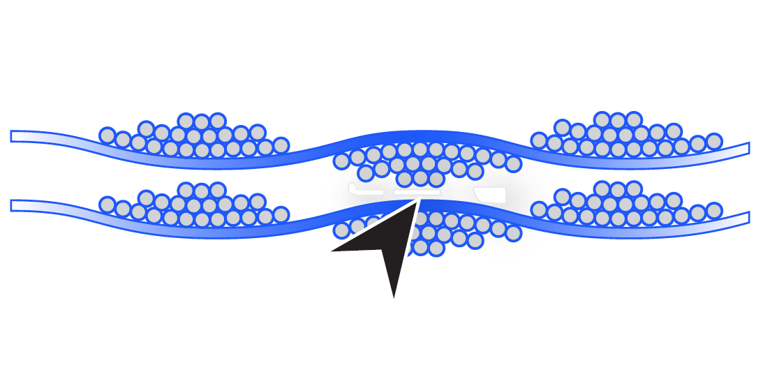
The IPC-6012F standard also specifies acceptability in terms of cavity floor or ceiling flatness, adherence of plating to cavity walls and other acceptability criteria. Type 2 and Type 3 cavities with plated cavity walls can exhibit voiding behind the cavity plating. The acceptability requirements in IPC-6012F provide limits on voiding for different product classes.
How to work with a fab vendor
The fabrication house can be a valuable resource when designing cavities into a PCB. Fabrication vendors should be consulted early regarding their capabilities, both in terms of fabrication tolerances in routing an embedded cavity, and in terms of etching clearances on the top and bottom copper layers that cap the cavity. Once these requirements are understood, the PCB layout can be designed to account for these tolerances.
Call out cavities in drawings
Embedded cavities need to be shown in fabrication drawings; this is done in a similar way to showing board cutouts and curved routes in the board outline.
- For arcs, show the routing path radius and angle
- List the floor and ceiling layers of the cavity
- Specify which design layers contain cavity outlines
Show cavity regions in design data
When the cavity is created in a PCB design tool, it should be drawn on a dedicated mechanical layer. Make sure to use a single mechanical layer to represent all cavities in a specific dielectric. If there are multiple cavities on different dielectric layers, then these should be drawn in different mechanical layers. Once these layers are created, they should be included in the design data exports. Cavities can also be shown in an ODB++ export if that is the preferred export format.
In the PCB layout editor, it’s critical to carefully match the cavity outline in the CAD data to the actual cavity drawing that will be fabricated. For Type 1 and Type 2 cavities, this is needed because the cavity can be mirrored as a keepout on the upper and lower copper layers, or it can be placed as an unfilled polygon object on these layers. A clearance rule should then be used to specify some minimum distance between etched copper features and the cavity region.
Tolerances and clearances
Once a cavity is placed into the PCB layout data, what kind of clearances and tolerances can be expected in the fabricated PCB? The cavity will be routed, so it should have the same tolerances as other routed features in a PCB – specifically board cutouts, slots and the board outline. Therefore, to account for these tolerances, the same clearances to the board outline or cutouts should be applied to the cavity region.
Outline tolerance
Typically this route tolerance will be up to +/-10 mils. Assuming Type 1 and Type 2 with no floor or ceiling copper, the clearance to the cavity wall should be at least as large as this board outline clearance. Due to etch tolerances for nearby copper features on the signal layers, it is good practice to add the etching tolerance to the board outline clearance. This will also ensure compliance with the acceptance requirements in the IPC-6012F standards and will account for any layer misregistration in rigid builds.
Depth tolerance
The flatness requirement in the IPC-6012F standard defines an expected tolerance in the depths of the cavity. The dielectric thickness needs to be sufficiently large to account for this variation in cavity depth, and the minimum thickness will depend on fabricator capabilities. Consult a fabrication house before selecting a dielectric thickness for the cavity layer.
Tradeoffs with other design characteristics
Due to the material thickness and clearance requirements near different types of cavities, there are certain tradeoffs that arise when including cavities in a PCB. Some of the most common design tradeoffs:
- Larger trace widths might be required on impedance-controlled buses due to material thickness requirements
- Large copper structures in fully metalized cavities can affect high-speed or RF signal propagation
- Material thickness requirements may limit sizing allowances, such as for blind or buried vias; or may limit where vias can be placed
Other factors such as cost, size, weight and performance tradeoffs arise in boards with large embedded heatsinks; in these boards, space and weight are at a premium and the increased weight may be undesirable. Consider the space savings, ease of layout and routing, added weight in the assembly, and processing costs before adding a cavity into the PCB.
Conclusion
Successful fabrication of embedded cavities in a PCB requires an understanding of industry standards and the capabilities of a fabrication vendor. If plans are to place a cavity in the PCB layout, determine the acceptable dielectric thickness, clearances and expected tolerances in the fabricated PCB. Finally, provide sufficient documentation for the fabrication house; early inquiry will help prevent mistakes, as well as streamline design and manufacturing processes.
Article originally produced by GlobalSpec, July 2023.
More articles
What is New in IPC-6012 Revision F?
IPC recently released an update to IPC-6012. Revision F covers qualification and performance specifications for ...
10 Causes of Lamination Voids and Ways Designers Can Prevent Them
One of the challenges in printed circuit board (PCB) manufacturing is the occurrence of lamination ...
Mastering Impedance Tables: A Comprehensive Guide for Designers
When it comes to designing PCBs (Printed Circuit Boards) and ensuring their successful fabrication, an ...