When it comes to designing PCBs (Printed Circuit Boards) and ensuring their successful fabrication, an often-overlooked but crucial tool is the impedance table. This table serves as a comprehensive guide that defines all the necessary requirements for your design in an easily accessible format. By providing a well-structured and clear impedance table, you can streamline the fabrication process, reduce questions from your fabricator, and minimize the risk of costly delays.
Understanding Impedance Tables
Before we delve into the tips for creating an impedance table, let’s briefly understand what it is and why it matters.
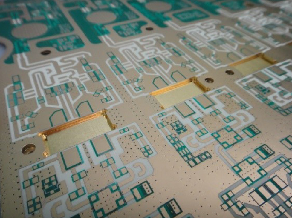
An impedance table is a document that outlines the essential electrical characteristics and requirements for your PCB design. It typically includes information related to trace width, spacing, dielectric materials, and impedance values for various signal layers. This table serves as a reference point for both designers and fabricators, ensuring that the PCB is manufactured according to the desired electrical specifications.
Why Are Impedance Tables Important?
1. Clarity and Communication: Impedance tables provide a clear and concise reference point for all stakeholders involved in the PCB design and fabrication process. This helps in effective communication between designers and fabricators, reducing the chances of misunderstandings or misinterpretations.
2. Minimizing Errors: By specifying all the necessary requirements in one place, impedance tables minimize the risk of errors during the design and manufacturing phases. This can save time, money, and resources in the long run.
3. Streamlined Fabrication: Fabricators can use the impedance table as a guide to ensure that the finished PCB matches the intended electrical characteristics. This streamlines the fabrication process and reduces the need for time-consuming back-and-forth communication.
Tips for Creating an Effective Impedance Table
Now that we understand the importance of impedance tables, let’s explore some tips for creating an effective one. Following are simple tips and definitions that can help you accurately complete an impedance table:
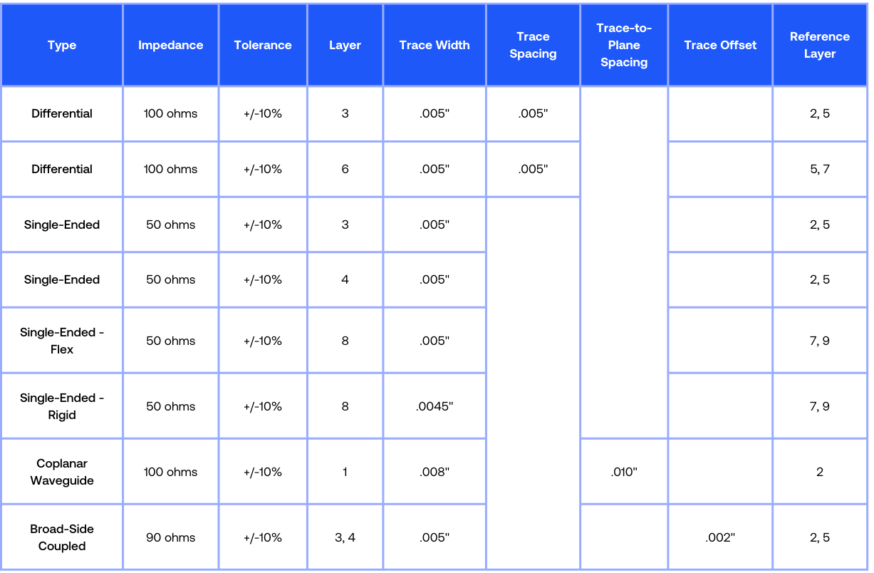
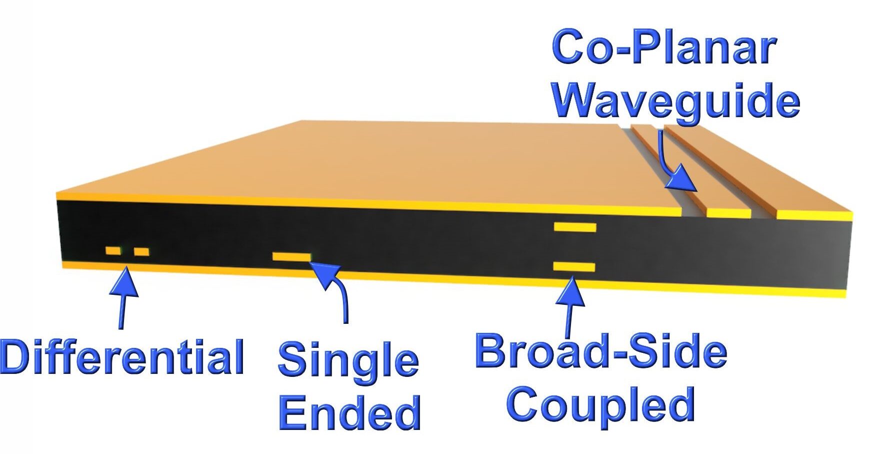
- Type: The impedance type notifies the fabricator what geometry to look for on the layers and what to model on the test coupon.
- Impedance: This column is for the nominal impedance values that are required per trace width, per layer.
- Tolerance: This is the tolerance on the nominal impedance value that will be accepted on the final product.
- Layer: Only the layers that contain the routed impedance traces should be listed on the table. Listing layers where the impedance trace widths aren’t present may delay a job.
- Trace Width: Ensure the trace width listed on the table matches the width that is routed on the design. The impedance traces should not be routed with the same width as the non-impedance-controlled traces.
- Trace Spacing: The trace-to-trace spacing for differential impedance should be listed.
- Trace-to-Plane Spacing: The trace-to-plane spacing for coplanar waveguide impedance should be listed.
- Trace Offset: The offset for broad-side coupled impedance should be listed. Best practice is to route the traces on the same core.
- Reference Layer: This column lists the reference planes in the design that should be modeled in the coupon, per impedance type.
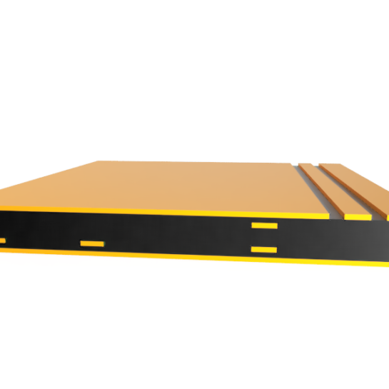
Example Table & Values
The examples below are not exhaustive, and only illustrate some of the common impedance types. For specific impedance questions, please reach out to your sales rep. or our FAE team (summit.fae@summitinterconnect.com) .
Conclusion
In conclusion, impedance tables are indispensable tools for ensuring the successful fabrication of PCB designs. By following the tips outlined in this blog post, you can create an impedance table that is clear, concise, and effective. This will not only help you avoid delays and errors but also enhance communication between you and your fabricator, ultimately leading to a smoother PCB design and manufacturing process.

More articles
What is New in IPC-6012 Revision F?
IPC recently released an update to IPC-6012. Revision F covers qualification and performance specifications for ...

10 Causes of Lamination Voids and Ways Designers Can Prevent Them
One of the challenges in printed circuit board (PCB) manufacturing is the occurrence of lamination ...
How to Thoughtfully Design Embedded Cavities into a PCB
The increasing demand for compact, high-performance and reliable electronic devices requires novel solutions to address ...