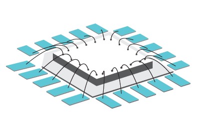
When they look at an integrated circuit, most people do not realize that what they are looking at is simply the package that encapsulates the actual IC or “the brains.” Integrated circuit packaging is something that happens to parts before they ever leave the manufacturing facility meaning that most designers and engineers never see the raw IC itself. Although the encapsulated IC may be the portion that brings value to the overall product, the package has an incredibly large effect on many different aspects of performance. While different packages are promoted by different manufacturers along with their specific pros and cons, this article will discuss the packages in general and the different attributes to consider when making a selection.
The IC itself is typically a small piece of silicon that somehow needs to be protected from and interfaced to the outside world. The package not only protects the semiconductor from mechanical stresses but also from environmental stresses, keeping it out of the elements and away from potentially corrosive or damaging materials. Some packages also provide a certain amount of ESD protection, further shielding the IC from potential damage. While the package protects and fully encloses the IC, it also must be able to interface with other devices. While there are different ways of doing this, the most common is via wire bonding. With wire bonding, a machine stamps a small piece of wire onto a nearly microscopic pad on the semiconductor before connecting that wire to the leads of the package. There are a few different ways the machine stamps the pad on, but the process generally involves pressure, heat, and ultrasonic waves to securely attach the wire to the surfaces.
How the IC is placed inside the package is also highly variable, with the cheapest and most frequently being the molded plastic method. Commonly, Dual-Inline Packages (DIPs) are enclosed in molded plastic. While low cost and mature as a technology, molded plastic has many trade-offs in terms of electrical conductivity and environmental protection.

Ironically, despite significant improvements over the years in the process of post-molded plastic packaging, the encapsulation process is also rather harsh. Other packaging types sometimes used are pressed ceramic and cofired laminate ceramic (both significantly more expensive than molded plastic), as well as chip on board (COB) technology. Done properly, pressed ceramic can create a hermetically sealed environment that will completely protect the IC from environmental factors. Cofired laminate ceramic is the most reliable packaging technology currently available on the market, making it ideal for avionics and military specs. COB actually dispenses with the packages completely and simply attaches the IC directly to a PCB. This PCB can be the final board that goes into the end product or it can have leads to connect it to either another PCB or another device.
As most consumer products use the plastic molded package material, the end designer’s bigger question is which package type to use. Dual inline, quad flat pack, ball grid array, thin shrink small outline – there are literally dozens of types of packages and hundreds of sub-categories within those types. The requirements for the project will narrow the choice down significantly, after considering the following characteristics:
- Heat dissipation – Larger packages are better at dissipating more heat and certain packages have specific pads or plates to help move heat away from the IC.
- High frequency – leadless packages are better for high frequency designs because the legs on other packages, particularly any through hole package, increase the inductance on the line and will likely change the apparent impedance.
- Ease of soldering – while surface mount and leadless packages tend to be smaller, this, in turn, makes them much more difficult to solder. Certain packages, such as the BGA, are nearly impossible to solder by hand, whereas a DIP package is trivial.
- Cost – DIP packages are relatively inexpensive due to the mature technology behind them. However, the increased amount of material means that in larger quantities, price breaks are not as generous.
- Mechanical stability – some environments can see parts shaken and bumped directly, at times physically removing the parts from the board. Through-hole parts are much better attached to the circuit board and can withstand greater abuse before failure.
- Size – smaller, portable devices require the absolute smallest packages feasible or the overall product becomes too large to be marketable.
- Pins – one of the reasons surface mount devices were developed is that the increasing number of pins on chips was making the chips unwieldy and grotesquely large. An upper limit was being reached. Surface mount devices, particularly BGAs, are better at fitting a large amount of connections into an incredibly small space.
- Standardization – most chips are packaged in a standard package type, making it very easy for designers to immediately know what he or she is dealing with, then create footprints or swap out parts.
Packages for IC’s have been instrumental in creating devices that can withstand the rigors of daily use. In addition to this protection, the packaging can increase design flexibility in how they are integrated into the final product, as well as can change the electrical characteristics of the IC, whether for better or for worse. The correct or incorrect selection of the package types can mean the success or failure of a project.


