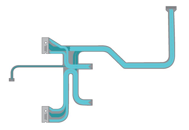
The three-dimensional capability of interconnects, along with the strength and stability for component placement and fixed hardware mounting, make rigid-flex boards an ideal solution for applications where space is limited. These boards allow conductor paths to be bent, twisted, or folded while maintaining electrical integrity, providing flexibility and compactness. Rigid-flex boards replace the need for hard-wiring rigid printed wiring boards (PWBs) together, occupying considerably less volume and reducing overall product weight. They offer an “all in one” interconnect solution for improved electrical performance, supporting double-sided component mounting. Additionally, these boards integrate the best capabilities of rigid and flex areas, providing maximum vibration resistance and a smooth transition between rigid and flex areas when mounting high-mass components.
Utilizing a single flex circuit instead of multiple hardboards, cables, and connectors leads to significant space and weight reduction. The inherent advantage of repeatable wire routing in flex circuits helps eliminate errors, ultimately reducing test time, rework, and rejects. The flat foil conductors in flex circuits dissipate heat more effectively and can carry higher currents than round wires of equivalent cross-sectional area. The conductor patterns in flex circuits maintain uniform electrical characteristics, allowing for the prediction and control of noise, crosstalk, and impedance. Additionally, flex circuits eliminate the need for color coding and bundling of wires, reducing the likelihood of assembly rejects and in-service failures.
Polyimide film, commonly in the form of Kapton Film, is the foundational material for flexible PCBs due to its excellent high temperature and electrical performance. However, the cost significantly increases for thicknesses above 2.0 mils.
The differentiation between Electro-Deposited (ED) and Wrought foils, classified as Type E or Type W, is fundamentally rooted in their material characteristics, influencing the suitability for rigid or flexible design configurations. In a comparative analysis, the nuanced examination of HA and HA-V2 special wrought foils against standard Rolled Annealed (RA) and Electro-Deposited (ED) foils involves evaluating specific technical parameters. This includes an in-depth assessment of electrical conductivity, mechanical strength, thermal properties, and flexibility, aiming to delineate nuanced distinctions that impact their performance in diverse applications and align with the specific requirements of stringent industry standards such as IPC-4204/11 and IPC-4204/1.
The careful selection of flex PCB materials, such as copper-clad laminates, polyimide films, and adhesiveless clads, plays a crucial role in determining the overall performance and reliability of electronic devices, adhering to industry standards like IPC-4204/11 and IPC-4204/1. Copper-clad laminates provide essential conductivity and mechanical strength, while polyimide films serve as the flexible substrate with excellent high-temperature and electrical performance. Adhesiveless clads eliminate the need for a bonding agent, reducing the risk of delamination and enhancing the overall structural integrity of the Flex PCB. Proper alignment with industry standards ensures that these materials collectively meet stringent criteria, guaranteeing robust performance and reliability in diverse electronic applications.
Dielectric films are pivotal in PCB fabrication, with their dielectric constant (Dk) and dissipation factor (Df) serving as critical parameters. The dielectric constant, or relative permittivity, influences signal propagation speed and impedance control, making low Dk desirable for minimizing signal distortion, especially in high-frequency applications. On the other hand, the dissipation factor (Df) gauges the efficiency of energy dissipation as heat within the dielectric material. Lower Df values are essential in high-frequency scenarios to reduce signal loss and enhance overall signal quality. Selecting dielectric films with precise and consistent Dk and Df values is crucial in achieving controlled impedance and reliable high-speed signal transmission in PCBs, emphasizing the importance of these distinctions in optimizing performance and signal integrity.
Coverlay, analogous to soldermask, is employed in encapsulating etched details on both flexible and rigid-flex products. Comprising a polyimide film coated on one side with a proprietary B-stage modified acrylic adhesive certified to IPC-4203/1, coverlay serves as a protective layer. Exposed features undergo pre-routing before bonding, ensuring precise encapsulation. An important consideration is that the adhesive thickness should exceed the copper thickness for optimal performance in the encapsulation process.
Incorporating laser-drilled microvias in a rigid-flex design enhances circuit density, and while design guidelines generally align with the rigid portion, there are some exceptions for the flexible area. The flexible section typically uses rolled annealed copper, presenting a challenge for laser drilling, necessitating larger laser vias for increased surface area. The recommended minimum microvia size is .012″ with a pad size of .006″ + over the microvia diameter. In the rigid area, the keep-out/transition area remains consistent with mechanical drill guidelines, emphasizing the avoidance of stopping a laser on rolled annealed copper foil. Additionally, for outer layers, it’s crucial not to encroach on the transition area with surface mount lands and features. These guidelines underscore the nuanced considerations for microvia implementation in both flexible and rigid sections of the PCB.
To protect flex materials during plasma, electroless copper, and copper plating processes, two methods are employed: the tape or open cavity approach and the cocoon or closed cavity method. The tape method, suitable for cases where the distance between the top of the rigid and the top of the flex is less than .013”, involves manual application and removal of Kapton tape before and after each plating process, necessitating additional cleaning steps. In contrast, the cocoon method, preferred whenever possible, utilizes a rigid cover laminated over flexible windows with a Teflon insert, providing a more streamlined process with less residue and requiring a minimum distance of .013” from the top of the rigid to the top of the flex. This approach enables efficient removal by a Z-axis NC router, enhancing the overall fabrication efficiency.
In flex PCB design, the bend radius recommendation is 10 times the material thickness for single-sided flex and 20 times for multilayer flex, with the potential for a 100x multiplier with thick copper and heavy adhesive. The adhesive thickness should surpass the copper thickness, and coverlay openings should be at least .010” per mil of adhesive over the pad size. It is advised to avoid right-angles in routed parts, opting for corners with a radius. Additionally, using a flexible epoxy bead at the rigid-flex interface is recommended, but it’s essential to note that the bead’s width will impact the available bend length.
In conclusion, adhering to IPC-2223 Design Guidelines is essential for a seamless PCB fabrication and assembly process. To optimize flexibility, all circuitry should be routed perpendicular to the bend, with no plated holes or vias in the bend area and none within 100 mils of any rigid-flex junction. Traces from flex sections should take a 45-degree bend upon entering the rigid section. It is crucial for the adhesive to be thicker than the copper foil, and to enhance bend radius in the flex section, unbonding flex cores can be considered. Additionally, incorporating a flexible epoxy bead at the junction of the rigid and flex sections is recommended for improved performance.
This article has been produced through the recording of the Flex Rigid Presentation. For more information listen to the recording here:
More articles

Summit Interconnect Welcomes Bobby Johnson as New Vice President of Human Resources
Shane Whiteside Appointed as New PCBAA Chair
Interview by Marcy LaRont I-Connect 007 ...

Summit Interconnect Announces the Appointment of David Lane as New General Manager and Vice President of Denver-based Advanced Assembly, A Summit Interconnect Company
Summit Interconnect Announces the Appointment of David Lane as New General Manager and Vice President ...