Due to our advanced operational capacity and nearly limitless flexibility, we can assemble more PCBs faster than anyone else in the industry.
Board Details
Standard
Advanced
Board Size
.25″ x .25″ minimum size, panelized
17″ x 21″
Processes
Our assembly facility utilizes the latest technology and equipment, and we always keep tabs on industry trends and customer demand to make sure our capabilities meet your PCBA needs.
Assembly Processes
Standard
Advanced
3, 5, and 10-Day Turns
Yes
Yes
Single-Sided SMT
Yes
Yes
Double-Sided SMT
Yes
Yes
Through Hole
Yes
Yes
No Clean
Yes
Yes
Clean / Wash
Yes
Yes
ROHS and Leaded
Yes
Yes
Additional Assembly Processes
Standard
Advanced
Press Fits
Yes
Yes
Box Build
Yes
Yes
Fine Pitch to 08 Mils
.08 Mils
.04 Mils
BGA Repair and Reball
Yes
Yes
Part Removal and Replacement
Yes
Yes
Underfill
No
Yes
Staking
No
Yes
Conformal Coating
No
Yes
Fencing and Shields
No
Yes
Components
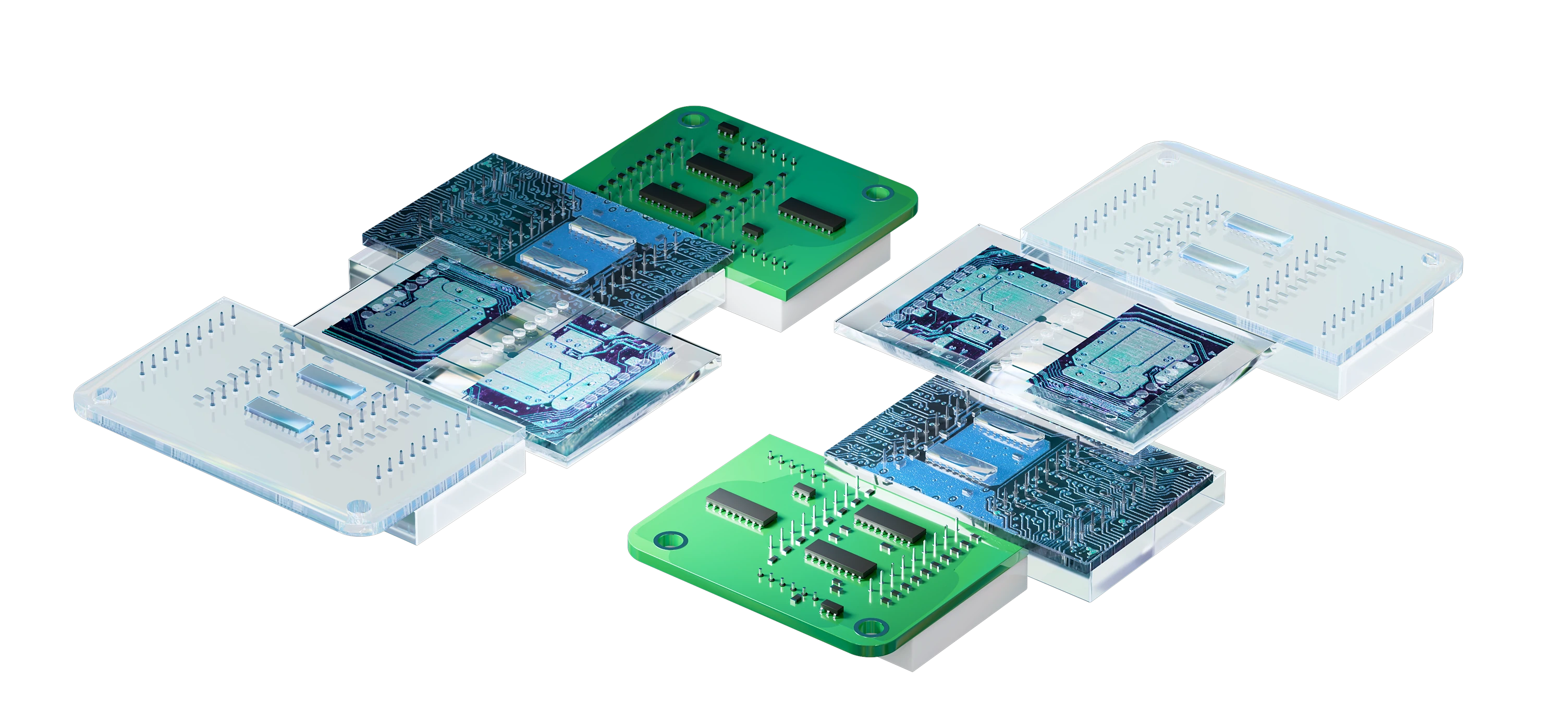
We provide full turnkey PCB assembly and manufacturing to help our customers across the country complete their projects on time. Our close and authentic partnerships with the most reputable US-based component and board suppliers is at the heart of the process. Test
Components
Standard
Advanced
SOIC
Yes
Yes
QFP
Yes
Yes
TQFN
Yes
Yes
Leadless
Yes
Yes
Through Hole
Yes
Yes
LGA
Yes
Yes
Passives
Down to 0201
Down to 01005
BGAs, uBGA, and VFBGA
Yes
Yes
Leadless Chip Carriers/ CSP
Yes
Yes
Microelescronics
Yes
Yes
Package-on-Package
Yes
Yes
Flip Chips
Yes
Yes
Hardware
No
Yes
Component Packaging
Standard
Advanced
Cut Tape
Yes
Yes
Loose Parts
Yes
Yes
Reels
Yes
Yes
Soldering Types & Methods
Soldering is one of the most basic techniques to understand for PCB assembly. Serving as a connective and conductive glue, a solid solder brings continuity and functionality to any circuit board.
Soldering Options
Standard
Advanced
Jet Paste Printing
Yes
Yes
Stencil/Water Soluble Paste
No
Yes
Vapor Phase Reflow
No
Yes
Conventional Reflow
Yes
Yes
Wave Solder / Selective Solder
Yes
Yes
Programmable Selective Solder
No
Yes
Inspection & Testing
Inspection is a critical part of the PCB assembly process. Without it, electronics manufacturers would never know for sure whether the PCB—and therefore the device—would work properly.
Inspection Processes
Standard
Advanced
Flying Probe
No
Yes
3D BGA X-Ray
Yes
Yes
Functional Testing
No
Yes
In-Line AOI
Yes
Yes
Visual Inspection
Yes
Yes
Component Inspection
Yes
Yes
Component Value Check
Yes
Yes
Ionic Contamination Test
No
Yes
Quality Standards
Following quality standards ensures all aspects of a PCB design are correctly implemented and the end products perform exactly as expected.
Quality Standards
Standard
Advanced
AS9100D
Yes
Yes
AS9102 FAIR
No
Yes
IPC Class II
Yes
Yes
IPC Class III
No
Yes
ITAR Certified
Yes
Yes
RoHS Compliant
Yes
Yes
Depanelization Methods
Once the boards are assembled and tested, they will need to be separated into their individual parts. There are many methods of depaneling PCBs, and which one you use depends on the type of panelization you chose.
Summit can fabricate PCBs ranging from simple 2-layer boards to highly complex designs with 30+ layers as standard, and emerging capabilities extend beyond 44 layers.
Standard maximum panel size is 18″ x 24″, with advanced capabilities up to 21″ x 24″ and emerging capabilities reaching 24″ x 36″.
Yes, Summit offers HDI layers and sequential laminations from 2-3 up to 7 layers as permitted by laminate type.
Summit specializes in advanced PCB technologies including laser micro vias, blind vias, buried vias, and via-in-pad, with options for non-conductive, conductive epoxy, and copper-filled vias.
Summit offers HASL (leaded and lead-free), White Tin, ENEPIG, ENIG, Immersion Silver, and Entek Plus HT/OSP finishes for both standard and advanced applications.
Yes, Summit provides full turnkey PCB assembly including single and double-sided SMT, through-hole assembly, BGA placement, and additional services like box build, conformal coating, and functional testing.
Summit Interconnect maintains comprehensive quality certifications including AS9100D, IPC Class II and III, ITAR registration, and RoHS compliance. Certifications vary by facility based on specialized capabilities.
View our completefacility certificationsor contact us to match your project with the right certified location.
For inner layers with 1/2 oz. copper, Summit can achieve .003″/.003″ trace width/spacing in advanced capabilities, with emerging capabilities below .0025″/.002″.
 Your connection to advanced PCB manufacturing