 Your connection to advanced PCB manufacturing

Before you layout a circuit, it’s generally a good idea to understand what is happening in your schematic. And before you lay out a schematic, it’s generally a good idea to understand what is happening in your block diagram.
Overview
Below is the basic block diagram for a circuit. The job of an electrical engineer is to determine how to make each of the blocks and each of the data buses work correctly without interfering with any of the other parts of the circuit. Each block is converted to a schematic.
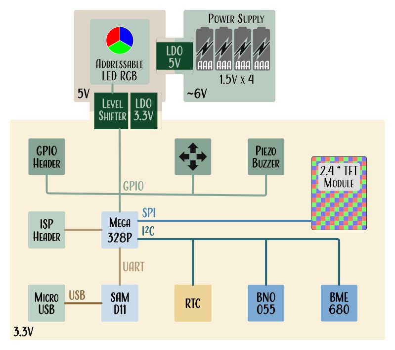
Power
The power in the circuit diagram above is delivered by batteries. The batteries feed a low-dropout (LDO) linear regulator that provides 5V to power the addressable RGB LEDs as well as a 3.3V LDO that powers the rest of the circuit. A logic-level translator will convert the Mega’s 3.3V logic outputs to 5.0V logic inputs.
Serial Data Bus
Four serial data buses are present in our circuit example and are used to transfer information.
- A Serial-Peripheral Interface (SPI) bus that communicates with the TFT module
- Universal Asynchronous Receive & Transmit (UART) that is used to program the microcontroller
- I2C that communicates with our sensors and Real-Time Clock (RTC) module
- A Universal Serial Bus that is used to communicate with an external computer for programming and debugging.
GPIO Pins
- Several pins will be used to command the Addressable RGB LEDs, read the status of push-buttons, and activate a piezo-buzzer.
Block Interaction
Blocks should be independently designed and connected to the main microcontroller. There are several common ways to do this such as with global nets and connector ports and hierarchical blocks. With hierarchical blocks, each circuit block is designed independently on a hierarchical page and then connected to the top-level via hierarchical connectors. In a hierarchical layout, only the connections between the blocks are shown on the top level (inputs, outputs, switch lines, etc…). Often times you’ll see power connections included as well.
Power System Overview
Unless you are a fan of fire, it is not a good idea to use multiple power sources at once. Engineers cannot depend on users to remember to disconnect one source before they connect another. Passive or active measures must be used to prevent multiple sources from powering the circuit at the same time. The simplest option is to use a break-before-make selector switch. Adding a switch increases the BOM cost, and mechanical devices are prone to failure.
Let’s take a look at the four options available for power sources: Nothing attached, only battery power, only USB Power, and both usb and battery power.
Option 1: Nothing Attached

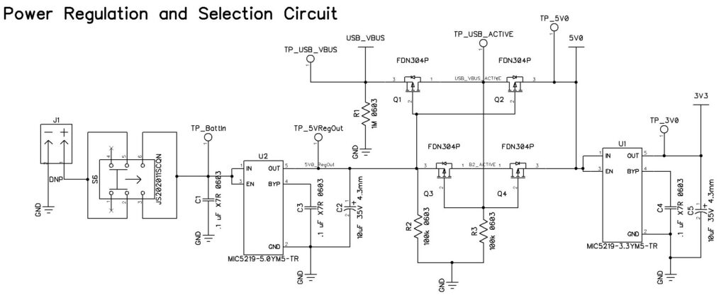
As you can imagine, nothing happens. P-channel MOSFETs behave as a normally closed (conducting) switch that opens (non-conducting) when a voltage is present at the gate. Since no voltage is present at the gate of Q1, Q2, Q3, or Q4, the “switches” are all closed and any current that arrives will be readily conducted.
Option 2: Only Battery Attached

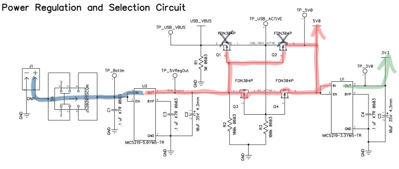
With the battery attached and the switch turned on, current flows through to the 5.0V LDO and through Q3 and Q4 to the 3.3V LDO and out to the rest of the circuit. R3 keeps the gate potential of Q3 and Q4 at 0V. At the same time, the gates of Q1 and Q2 are energized, stopping reverse conduction of current through the circuit.
Option 3: Only USB Attached

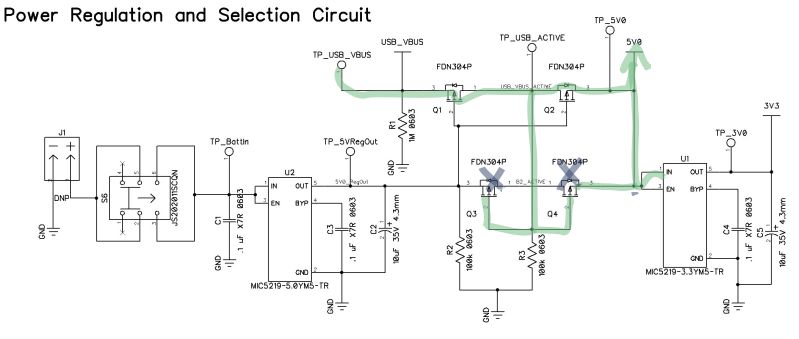
With the USB power connected, R2 keeps the gate of Q1 and Q2 and ground potential, which keeps Q1 and Q2 conducting current between the source and drain. At the same time, the gates of Q3 and Q4 are connected to the net that connects Q1 and Q2, closing the conducting paths between Q3 and Q4 drain and source, which prevents the backward flow of current.
Option 4: Both Sources Attached

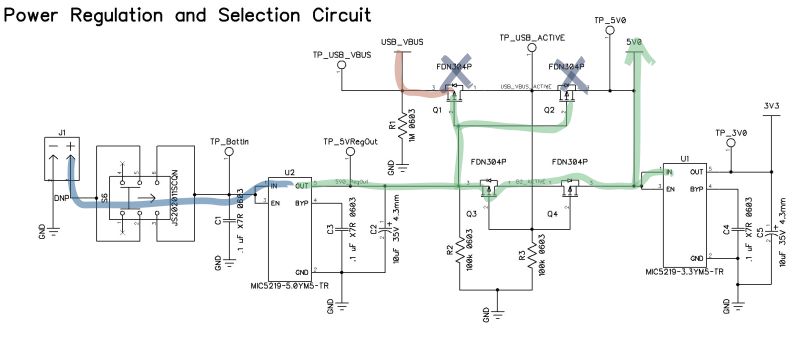
When both sources are energized, the 5.0 V LDO generates a potential difference at the gates of Q1 and Q2, shutting off the conduction path across the drain and source, stopping USB_VBUS current before it ever gets a chance to enter the rest of the circuit.
Summit Interconnect, Inc. is pleased to announce the acquisition of ITL Circuits.
Established in 1971 and located in Toronto, Canada, ITL Circuits is one of North America’s leading providers of printed circuit boards. The oldest and largest privately held PCB manufacturer in Canada, ITL Circuits provides a significant expansion of Summit’s operations in North America.
ITL Circuits is AS9100, NADCAP and MIL-PRF 31032 certified and has a long history of servicing military programs for the Canadian Department of National Defense (DND) prime contractors and Australian Defense Force (ADF) primes. ITL Circuits is also a long time supplier to the United States DOD prime contractors under U.S. ITAR 126.5 under the Canadian Controlled Goods (CGP) exemption.
Shane Whiteside, President and CEO of Summit Interconnect, Inc. stated, “ITL’s capabilities complement Summit’s and will provide additional volume manufacturing capacity across a broad range of technology. The additional and meaningful scale will further strengthen our ability to serve our customers and broaden our relationships with key suppliers. This is very exciting news for both Summit and ITL and we welcome our new Toronto employees to the Summit team.”
About Summit Interconnect: Summit Interconnect is a leading manufacturer of advanced technology printed circuit boards. Manufacturing services include quick turn, prototype and production through our advanced technology facilities located in California and Toronto, Canada. For more information, please go to summit-pcb.com
About ITL Circuits: ITL Circuits is one of North America’s leading providers of printed circuit board fabrication services. Established in 1971, ITL Circuits is highly certified and is the oldest and largest privately held PCB manufacturer in Canada. ITL Circuits serves both original equipment manufacturers (OEM) and electronic manufacturing services (EMS) companies with advanced technology prototype and production PCB’s around the globe. For more information, please go to: itlcircuits.com