Backdrilling in Circuit Board Fabrication: Enhancing High-Speed Signal Integrity
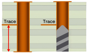
Backdrilling is used in printed circuit board (PCB) fabrication to remove unwanted via stubs, which can cause signal integrity issues in high-speed designs. When a signal travels through a via, any unused portion, known as a stub, can create reflections and distortions, leading to insertion loss and potential data errors. This problem becomes more severe at higher data rates. For example:
- When the data rate increases from 3 Gb/s to 6 Gb/s, the distortion doubles.
- At even higher speeds, unaddressed via stubs can completely degrade the signal, rendering the circuit unreliable.
Backdrilling selectively removes these stubs by drilling just deep enough to eliminate the excess via length while preserving the functional electrical connections. This process is essential in high-frequency applications, such as telecommunications and data centers, where minimizing signal degradation is critical for optimal performance.
The Backdrilling Process
The process starts with identifying vias that require backdrilling based on signal integrity analysis, followed by carefully aligning the PCB for precision drilling. The drill bit is then set to a controlled depth, typically leaving a minimal stub of 0.005”/.127mm to avoid over-drilling. Once completed, the backdrilled vias are inspected to verify accuracy and ensure optimal signal performance. This technique is widely used in high-speed PCB designs to reduce signal reflections, improve impedance matching, and enhance overall circuit reliability.
Back Drill Tolerances
A key consideration in the backdrilling process for PCBs is maintaining precise back drill tolerances, as even slight variations can impact signal integrity and overall board performance. Back drill depth tolerance is typically ±0.002 inches, ensuring that the stub is minimized without over-drilling into the functional layers.
Additionally, the back drill hole size must be carefully controlled—industry standards recommend a back drill diameter 0.010 inches larger than the plated-through-hole (PTH), while emerging technologies allow for even smaller sizes, down to 0.008” inches or less.
IPC-6012 Revision F Requirements
IPC-6012 rev F requires that the finished product must have 1 hole in the X & Y axis per panel for each back drill depth to validate that the back drill is conforming.
Recommendations for Achieving Back-Drilled Plated Vias
- Most backdrilled plated vias are epoxy filled. While this is not necessary, the quality of the back drill is more consistent. Non-filled holes can be plugged with debris that is difficult or impossible to remove. Plugged holes could cause assembly issues
- The diameter of the back drill is typically .010″/.25mm larger than the original drill bit size that created the plated via. It is important that designers know the actual drill diameter that your fabricator will use. The oversize based on the original drill bit size will be needed to determine safe keep back distance to copper features near the back drill.
- The smallest recommended back drill diameter is .018″/.45mm; anything smaller tends to break, resulting in a scrapped part. For example, if the original via is drilled at .010″/.25mm the back drill diameter will be .020″/.5mm.
- Once the actual back drill bit size is determined, the layout must have the additional safe space required from the back drill to a conductor of a different net. This space should be .010″/.25mm or greater, but can be .008″/.2mm with additional safety concerns. Many CAD systems have difficulty adding the extra space so be vigilant in your designs.
- Specify stub length. Standard stubs should be .010″/.25mm +/-.003″/.075mm, and advance designs can be .005″/.25mm +/-.002″.05mm. It is not possible to have a zero length stub, if the back drill stopped on the desired layer the barrel/pad interface integrity would be compromised.
Recommendations for the Side and Depth of the Back Drill
Clearly state the side that the back drill starts from. Top side or bottom side for each back drill span required.
- Provide a drill program for back drilling and a drill chart with counts. Don’t leave it to the fabricator to determine. A guessing fabricator can create opens or bad back drill depths that have stubs longer than desired.
- Specify the “Don’t Cut Layer” in the back drill. For example, if we have a 10-layer PCB and we are back drilling from the bottom side of the PCB. The goal is to have a connection from layers 1-4, the fabrication drawing should specify Back drill from bottom side DON’T CUT LAYER 4″. Let the fabricator specify the distance.
- Don’t Specify “Stop between layers X and Y. Specify the DON’T CUT LAYER and the stub length.
Don’t Specify the distance, the fabricator will figure this out in the determination of the stack up and the design data.
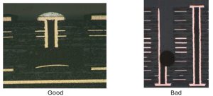
- Last one and this one can be kind of confusing. There needs to be a minimum distance of .010″ of dielectric between the outside layer to the closest DON’T CUT LAYER. This is necessary to have sufficient drill depth (.005″./.13mm minimum) to remove the plated barrel, with a target safe distance to the DON’T CUT LAYER. (.005″/.13mm). If shorter than .010″.25mm several bad things can happen. There can be a burr of copper to the outer surface that causes a short and will only be detected after final system assembly. Or, the drill has gotten too close to the DON’T CUT LAYER and the net has an open typically after assembly. Here is an image that demonstrates this concern.
- Designs can have many depths from both sides of the PCB but PCB pricing is based on the different depths and overall quantity of back drills

Advancements in Backdrilling Technology
Advanced drilling systems utilize high-precision linear drive motors, which enhance drill accuracy by providing smoother, more controlled movement, and minimizing mechanical errors during the drilling process. Additionally, optical registration technology ensures precise alignment of the drill with the target vias, reducing misalignment issues and improving overall consistency. By integrating these advanced features, manufacturers can achieve tighter tolerances, minimize via stubs more effectively, and enhance signal integrity in high-speed PCB designs.
Conclusion
As PCB technology advances, innovations in drilling precision and alternative solutions continue to refine the process, ensuring optimal functionality for next-generation electronic devices. For PCB designers and manufacturers, understanding and implementing effective backdrilling techniques is key to achieving high-performance, reliable circuit boards.
More articles
Where PCBs Are Born: Touring a Quick-Turn Factory in North America
This article was originally published by Hardware FYI. ...

Orbital High Ground Why Space Superiority Is Slipping Away
“The next war might be won—or lost—22,000 miles above Earth.” That’s not science fiction. It’s the ...

RF & Microwave PCB Design: Navigating High-Frequency Complexity with Precision
RF and microwave PCBs aren’t just signal carriers—they’re performance enablers. In the GHz realm, every ...