Your connection to advanced PCB manufacturing
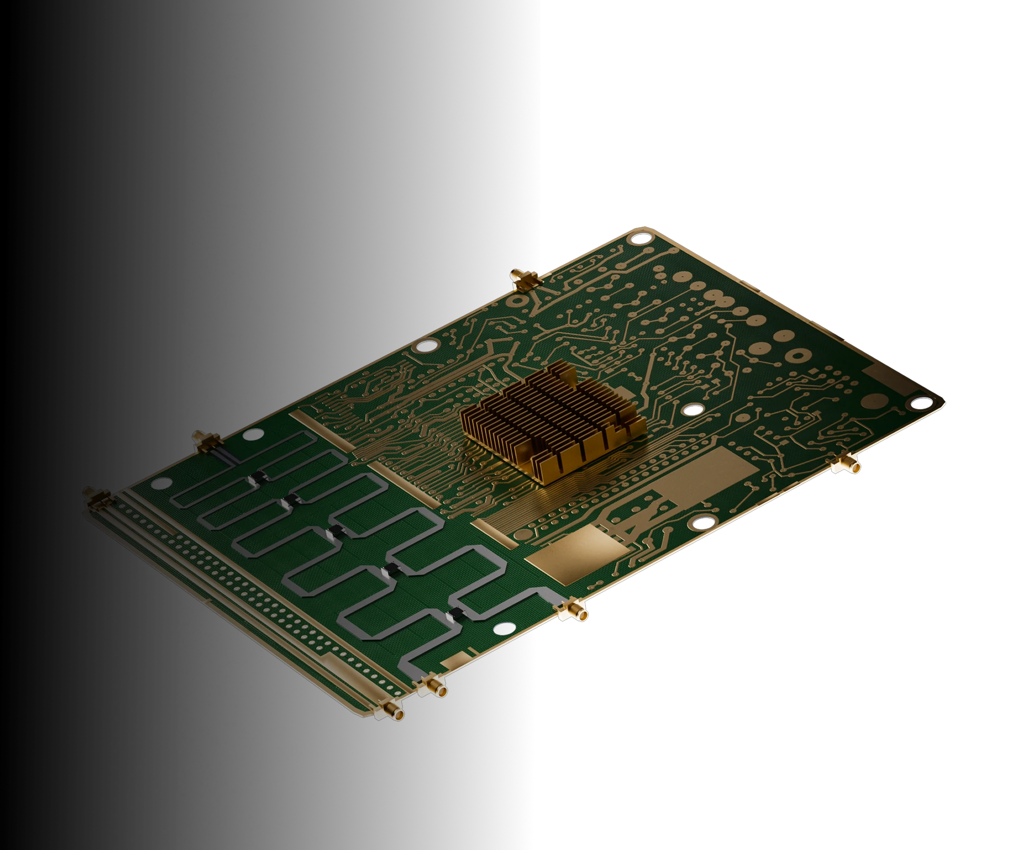


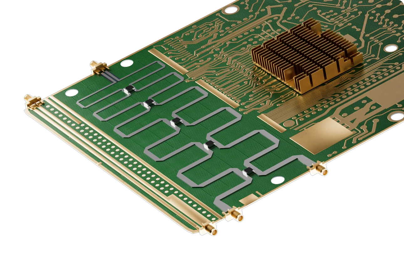
RF and microwave PCBs are designed to operate at frequencies from ~100 MHz to 30 GHz (RF) and beyond 30 GHz (microwave), where signal loss, impedance stability, and dielectric performance are critical. They require specialized laminates such as Rogers, Taconic, Arlon, or PTFE composites with controlled dielectric constants (Dk) and low dissipation factors (Df). Fabrication must maintain precise impedance control per IPC-6018 to ensure minimal reflection and phase distortion.
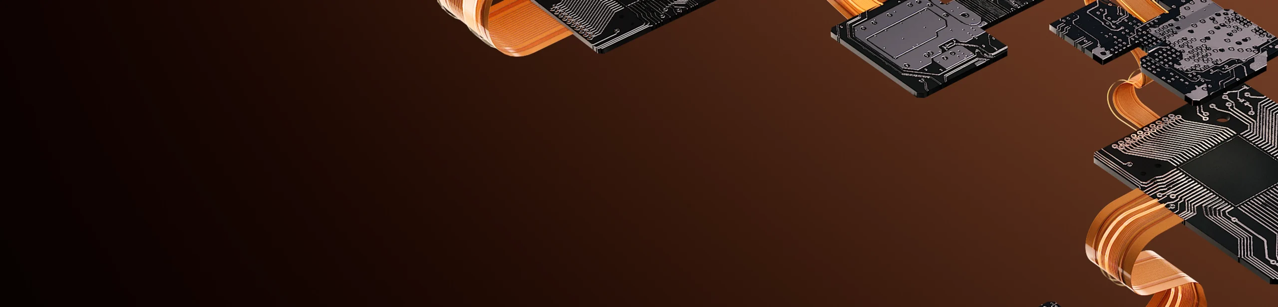
High-Performance RF and Microwave PCBs
RF circuits have moved from large mil-aero applications into a rapidly growing range of commercial products. Smaller boards with RF/microwave circuits on board are substantially more complex, requiring a PCB manufacturer with Summit’s expertise.
Reliable Manufacturing for High-Frequency Designs
RF and Microwave PCBs require precise materials and manufacturing to support high-frequency performance, low signal loss, and controlled impedance.
With deep expertise in PTFE and low-loss laminates, precision drilling, and advanced modeling, Summit delivers reliable RF and microwave boards that meet demanding electrical specifications for signal integrity, power handling, and manufacturability.
RF / Microwave PCB key attributes
- Low-loss laminates minimize attenuation at high frequencies.
- Controlled impedance ensures consistent signal performance.
- Precision drilling supports plated through-holes and tight tolerances.
- Advanced modeling optimizes stack-ups for RF designs.
- Reliable fabrication maintains performance across wide frequency ranges.
Designing for RF & Microwave Performance
Successful RF and microwave designs require more than just the right materials. These boards require precise modeling, careful layout, and rigorous process control. Small variations in dielectric properties, trace geometry, or via construction can significantly affect signal behavior at high frequencies.
Our engineering team partners with customers early, using simulation and stack-up optimization to ensure manufacturable designs.
Design-Focused Attributes
- Careful stack-up planning reduces insertion loss and reflection.
- Tight process controls maintain dielectric and copper consistency.
- Precise via design minimizes parasitic inductance and capacitance.
- Simulation tools validate impedance and signal performance.
- Collaborative engineering streamlines design-to-fabrication handoff.
Capabilities
RF/Microwave capability hightlights.
-
Wide Range of High-Speed, Low-Loss Materials
Essential for minimizing insertion loss and dielectric variability. Summit's expertise in PTFE, hydrocarbon, and hybrid laminates ensures stable performance across GHz and mmWave frequencies.
-
Tight Tolerance Stripline & Controlled Impedance
Critical for consistent signal behavior in high-frequency circuits. Our precision imaging and process controls deliver repeatable impedance within tight tolerances.
-
HDI/PTH Mode Suppression
Summit's advanced via design and suppression techniques improve signal integrity in dense RF layouts.
-
Plated Cavities and Edges
Enable embedded components, filters, and RF shielding. Proven cavity plating and edge processing support complex RF and microwave architectures.
-
Controlled Depth Milling
Precision features for connectors, waveguides, and RF transitions. Advanced milling processes maintain accuracy for critical RF geometries.
-
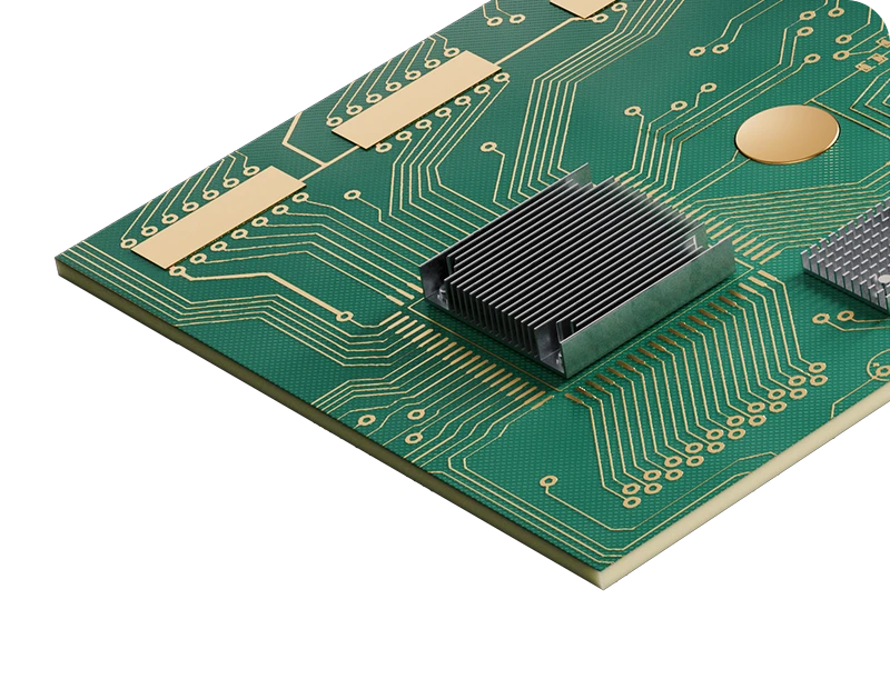
Bonded Heat Sinks
Manage thermal load in high-power RF designs. Summit's ability to integrate metal-backed substrates and bonded sinks ensures thermal reliability without compromising performance.

High Speed and RF Designs
Learn important concepts for RF and high-speed digital designs, materials for RF, and more.
Contact us
We’re available to answer any questions
-

Email Us
info@summitinterconnect.com -
Call Us
+1 (877) 264-0343
FAQ
Frequently asked questions.
-
-
Controlled impedance is achieved through tight control of trace width, dielectric thickness, copper plating, and laminate Dk. Summit uses advanced CAM modeling and in-process testing to hold tolerances within ±5% per IPC-6018 Class 2 or 3. Ground plane integrity, uniform copper distribution, and proper stack-up modeling are essential to maintaining impedance over temperature and frequency ranges.
-
For frequencies above 1 GHz, low-loss materials such as Rogers RO4350B, RO3003, Taconic RF-35, and PTFE-based laminates are preferred. These materials provide stable Dk across a wide temperature range, low insertion loss, and minimal moisture absorption. IPC-4103 specifies base materials for high-speed/high-frequency PCBs, guiding dielectric and thermal performance requirements.
-
Losses are minimized through smooth copper foils (low profile to reduce conductor loss), minimal via transitions, back-drilling of unused stubs, and optimized ground return paths. Plated through-holes and vias are modeled to avoid parasitic inductance, and transmission lines are routed with consistent geometry to meet IPC-2221/IPC-2222 design rules for high-frequency performance.
-
Summit performs network analyzer measurements, time domain reflectometry (TDR), and S-parameter characterization to verify insertion loss, return loss, and impedance stability. Testing is done in accordance with IPC-TM-650 methods and IPC-6018 performance specifications, ensuring compliance for aerospace, defense, telecommunications, and high-reliability commercial applications.
Solutions
We manufacture a broad range of PCB types and technologies for a one-stop solution
-

Thermal Dissipation PCBs
Summit Interconnect manufactures thermal management PCBs with advanced materials and processes that optimize heat dissipation for reliable performance in demanding, high-power applications.
-

High-Density Rigid
Summit provides HDI rigid PCBs with microvias, blindburiedvias, back drilling, via fill, metal core, and large panel options.
-
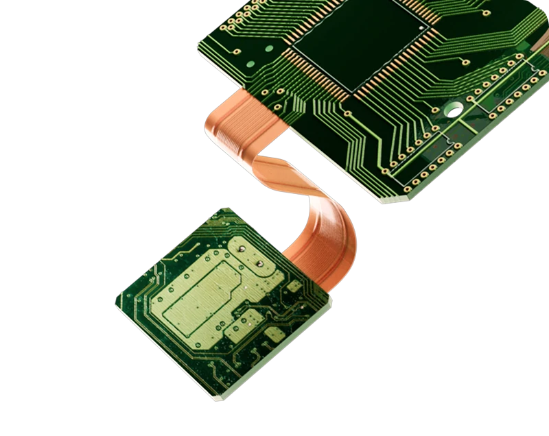
Rigid-Flex and Flex
As experts in rigid-flex and flex manufacturing, we handle rigid-flex, bookbinder, multilayer, adhesiveless & adhesive, stiffeners, laser ablation, thin flex laminates, assembly options and more.
-

Prototype Assembly
Looking to test your design before committing to a full PCB production run? Small-quantity prototype PCBs are manufactured with the same state-of-the-art equipment and quality processes used for production runs.


Resources
Additional RF resources
-
Dec 16, 2025
RF & Microwave PCB Design: Navigating High-Frequency Complexity with Precision
-
Dec 16, 2025
PCB Design Annular Ring
-
Dec 16, 2025
Driving PCB Innovation with Advanced Materials and Automation
-
Dec 16, 2025
From Layout to Fab: Gerry Partida’s Top DFM Guidelines for PCB Designers
-
Dec 16, 2025
Squeeze Every Last Mil. Out of Your Next Panel Design
-
Dec 16, 2025
The Process of Panelizing in PCB Manufacturing and Prototypes