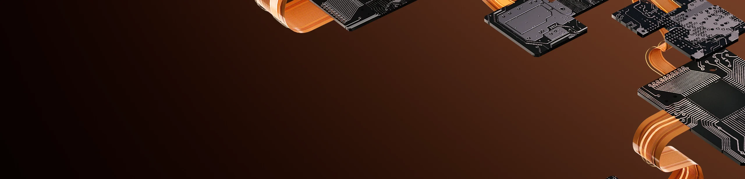
Your connection to advanced PCB manufacturing


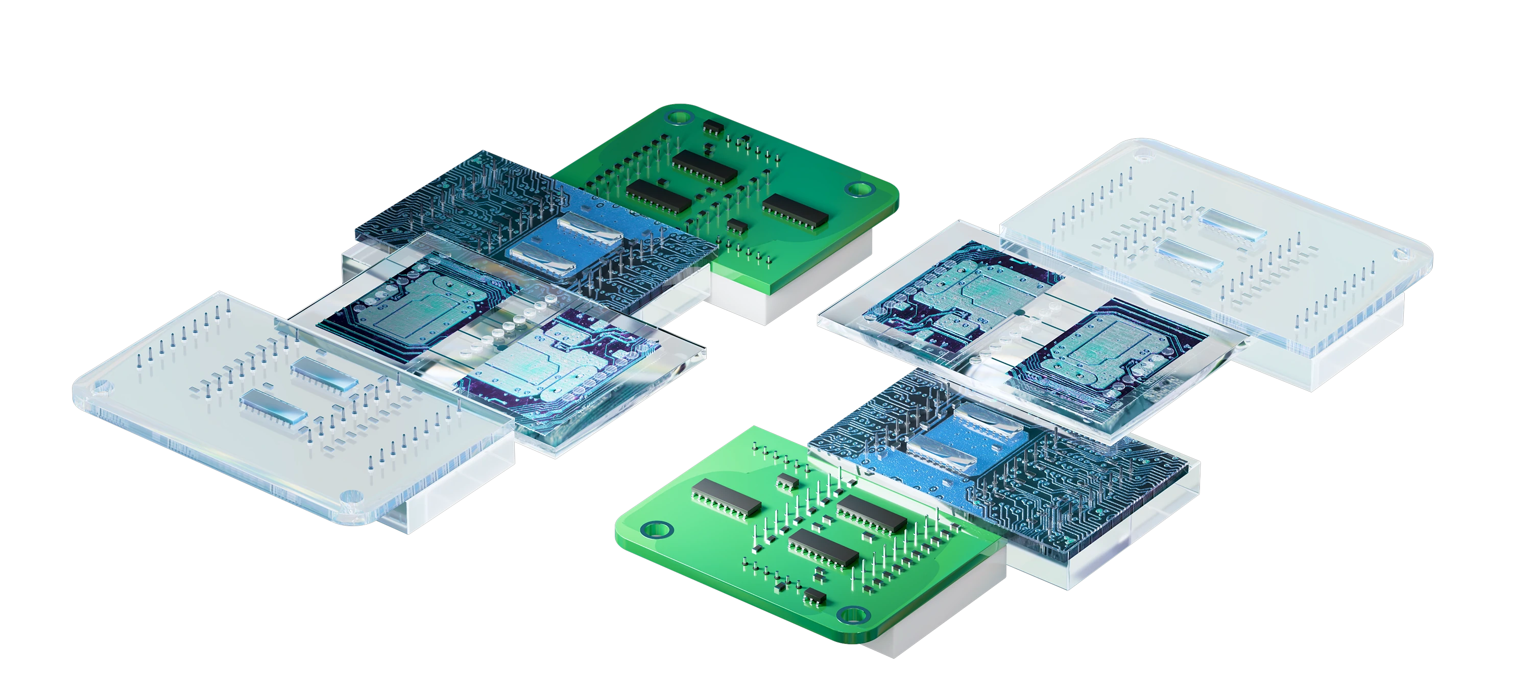
Vias are critical to achieving high interconnect density, especially in HDI designs. Summit uses microvias, blind and buried vias, and via-in-pad structures to route complex circuits within tight spaces. These features reduce signal path length, improve electrical performance, and allow for higher component density without increasing layer count.
Standard to Advanced Rigid PCBs
Summit’s integrated network of facilities manufactures rigid and high-density interconnect (HDI) PCBs, from simple multilayer designs to complex builds for mission-critical performance.
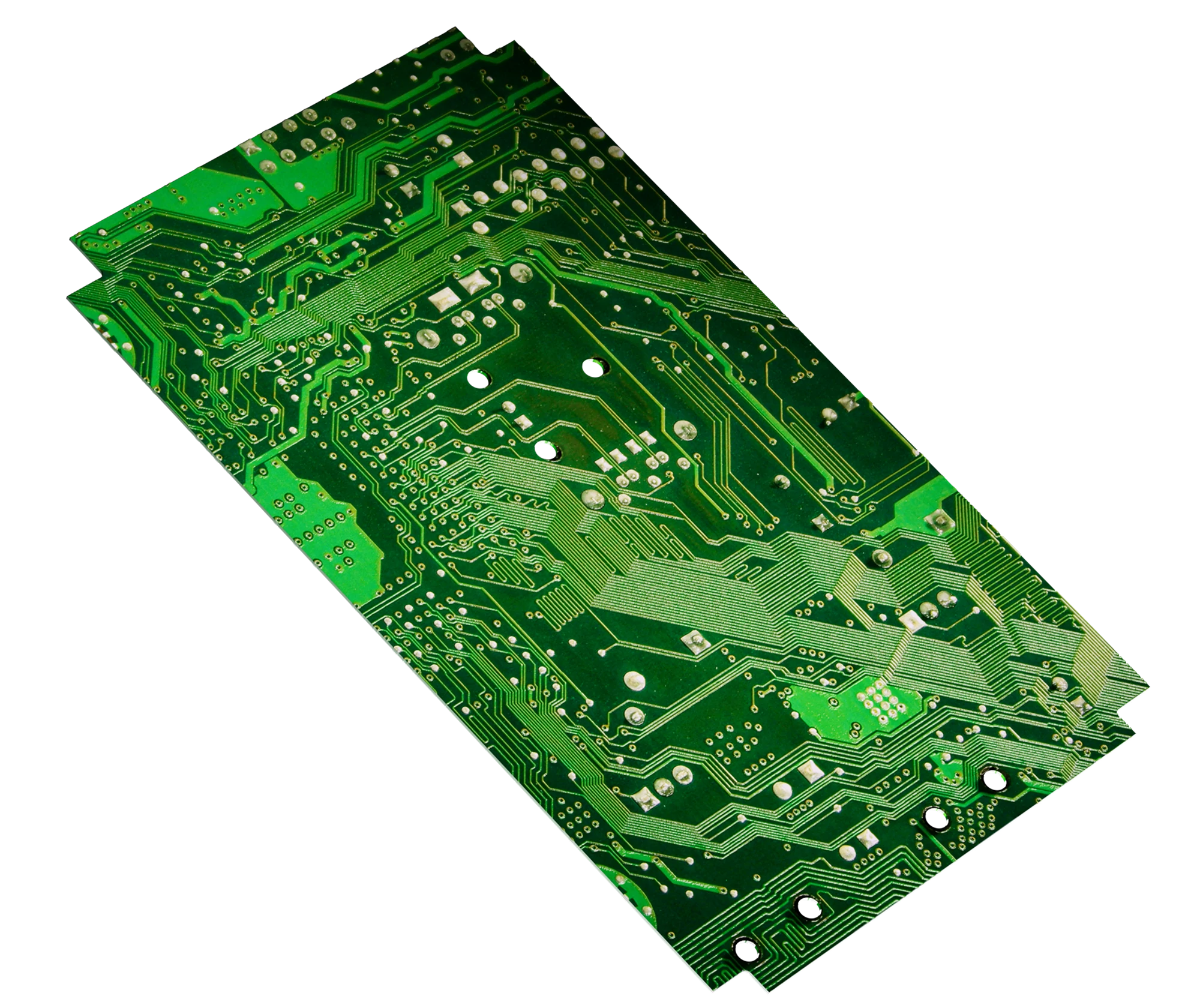
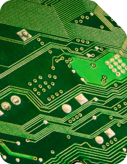
Standard Rigid Printed Circuit Boards
Built on proven dielectric materials such as FR4, core rigid PCBs provide stable mechanical support, reliable electrical performance, and straightforward manufacturability. These boards are the cost-effective choice for designs that don’t require extreme density or advanced interconnect structures.
With decades of rigid PCB experience, Summit delivers consistent quality across simple through-hole boards to complex multilayers across all industries.
Key Attributes of Core or Standard Rigid PCBs
- Stable performance with FR-4 and other standard dielectric cores
- Through-hole via structures for straightforward interconnect
- Scalable from single-sided to high-layer-count designs
- Predictable thermal and electrical characteristics
- Cost-effective solution for mainstream applications
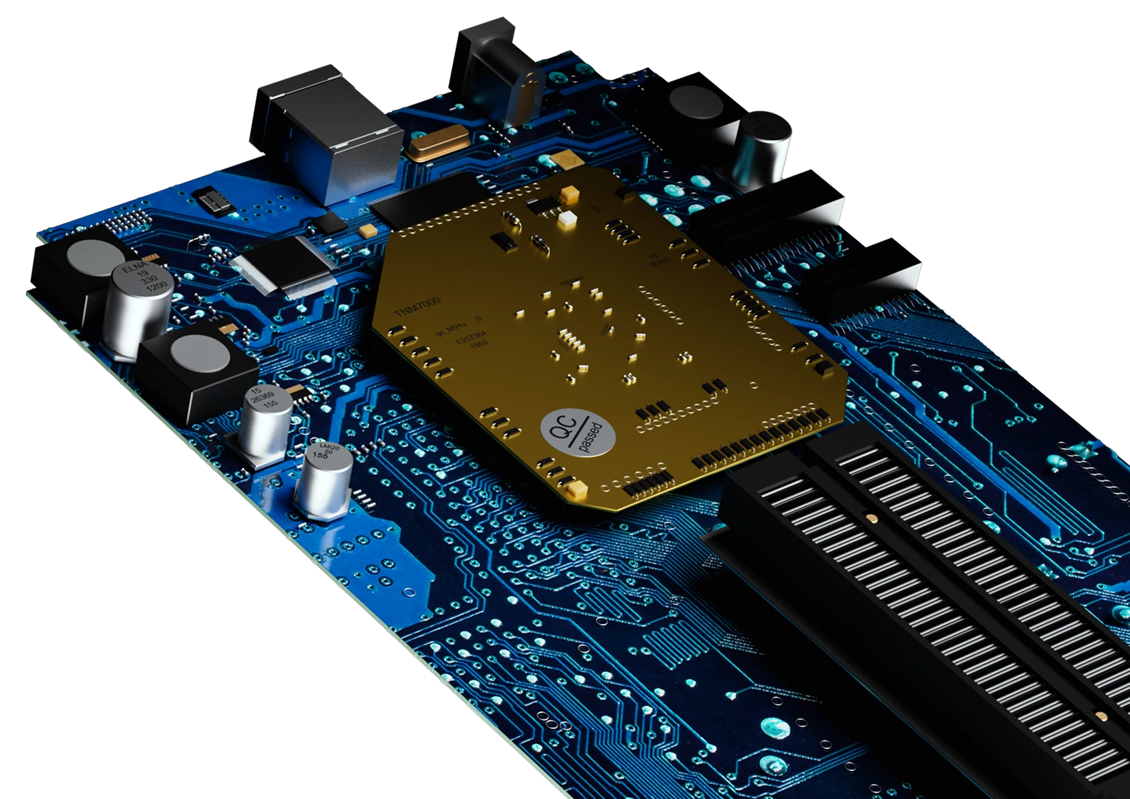
Advanced, High-Density
Interconnect (HDI) PCBs
Advanced HDI PCBs enable miniaturization, higher I/O density, and improved electrical performance through microvias, blind/buried vias, and sequential build-up layers.
With advanced laser drilling, sequential lamination, and fine-line imaging, Summit delivers precise, high-density boards. Our engineering teams work closely with customers to optimize stack-ups for scalable, manufacturable designs that meet performance demands.
Key Attributes of HDI Printed Circuit Boards
- Microvia and build-up technology for high interconnect density
- Fine trace/space rules supporting fine-pitch and high-pin-count devices
- Improved electrical performance through shorter signal paths
- Flexible layer stack-ups to balance size, performance, and reliability
- Trusted for aerospace, defense, medical, and high-speed communications
Capabilities
Rigid PCB capabilities highlights
-
Blind, Buried, and Microvia Structures
Enable dense interconnects without sacrificing board space. Summit features precision laser drilling for stacked and staggered microvia designs.
-
Sequential Lamination for Complex Stack-Ups
Support higher layer counts and advanced build-up structures. We specialize in multiple lamination cycles executed with tight process control.
-
Back-drilling and Stub Removal
Improve high-speed signal integrity by eliminating via stubs. Advanced equipment deliver cleaner signals in high-frequency applications.
-
Via Fill (Conductive and Non-Conductive)
Increase reliability, assembly yield, and flatness for fine-pitch components. Summit is experienced in via fills for HDI requirements.
-
Specialty Materials and Oversized Panels
Optimize performance with the right dielectric, PTFE, or hybrid laminate. We offer broad material expertise and oversized panel formats.
-
Impedance Control and DFM Support
Ensure signal integrity and manufacturability. Summit's in-house modeling, simulation, and collaborative engineering improve first-pass yield.

Ultra HDI: The Next Frontier in PCB Design
Discover what ultra HDI is, why it matters, and how it’s shaping the future of PCB technology.
Contact us
We’re available to answer any questions
-

Email Us
info@summitinterconnect.com -
Call Us
+1 (877) 264-0343
FAQ
Frequently asked questions.
-
-
The annular ring is the copper pad area surrounding a drilled hole, and maintaining precise dimensions is essential for electrical and mechanical reliability. Summit’s laser and mechanical drilling processes, combined with tight registration control, ensure annular ring integrity in accordance with IPC-6012 Class 3 requirements, even on microvia and fine-pitch designs.
-
HDI PCBs support higher signal speeds by shortening trace lengths, reducing parasitic inductance, and enabling controlled impedance routing. This is critical for high-frequency and high-speed digital designs used in computing, telecommunications, and advanced electronics.
-
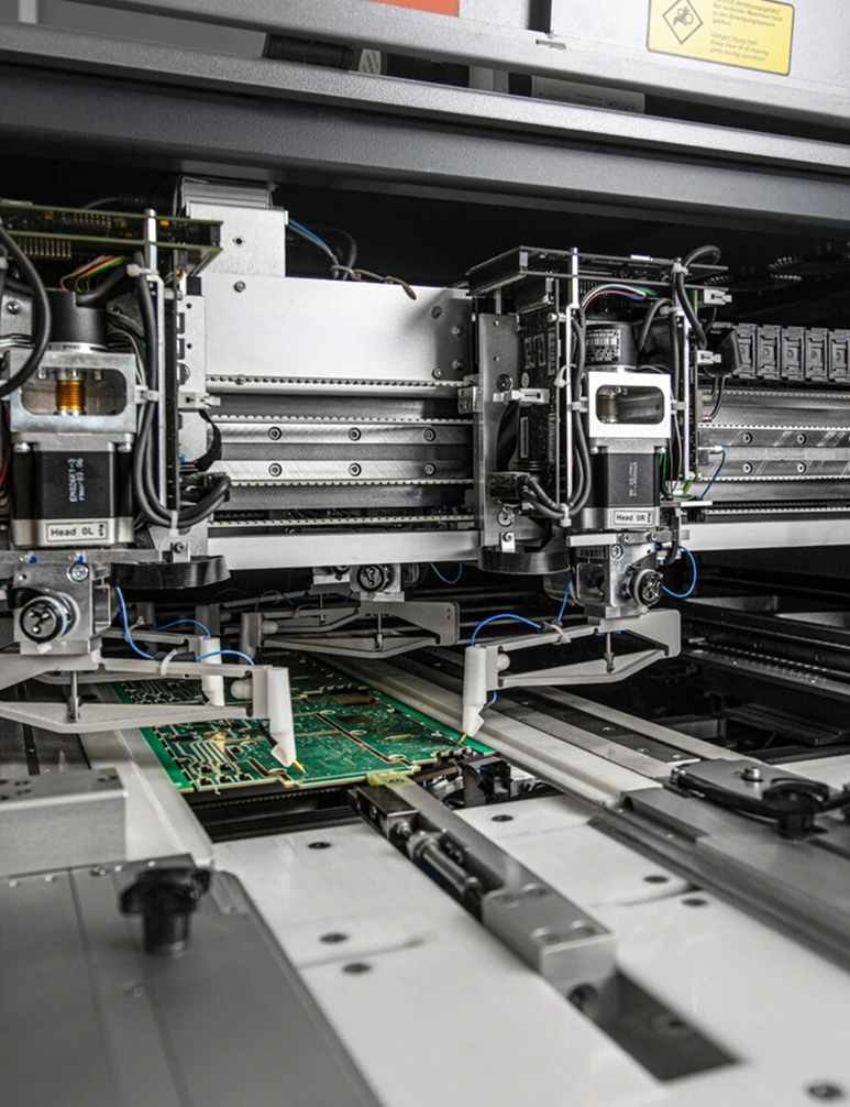
Building an HDI PCB often requires multiple sequential lamination cycles, laser drilling, copper filling, planarization, and precise imaging for fine-line features. Each step must be tightly controlled to maintain dimensional accuracy and electrical performance, especially for mission-critical applications.
-
We follow lean manufacturing principles, minimize scrap through precise process control, and use IPC standards to reduce rework and waste. By optimizing yields on complex builds, Summit supports both operational efficiency and environmental responsibility.
Solutions
We manufacture a broad range of PCB types and technologies for a one-stop solution
-

Rigid-Flex and Flex
As experts in rigid-flex and flex manufacturing, we handle rigid-flex, bookbinder, multilayer, adhesiveless & adhesive, stiffeners, laser ablation, thin flex laminates, assembly options and more.
-

RF / Microwave
We specialize in semiconductor reference cards, probe cards, DUT, and burn-in-boards. Our RF capabilities include high aspect ratio, low-loss materials, bondable gold, tight tolerance drilling, and sintering.
-

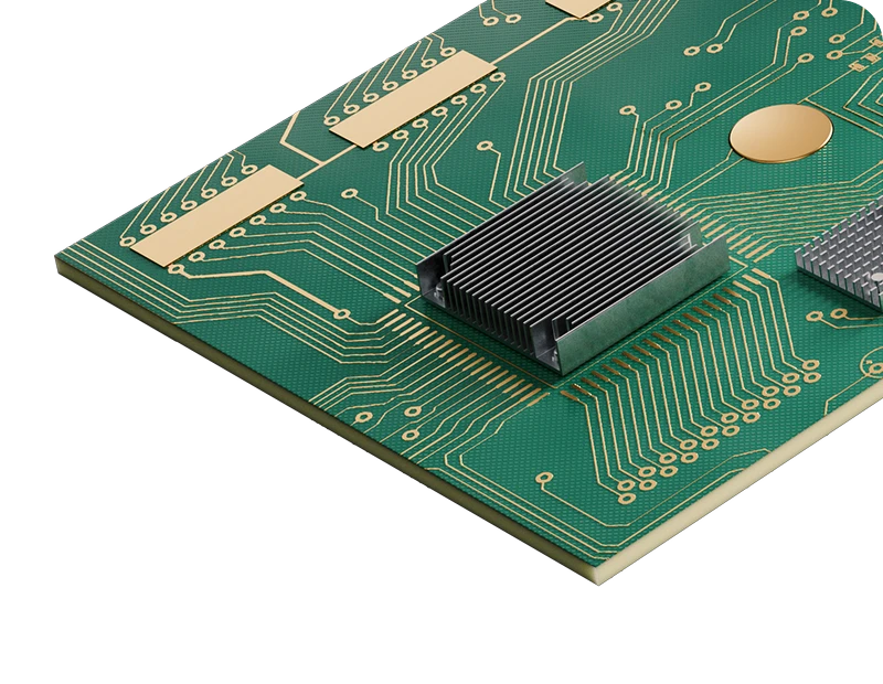
Thermal Management PCBs
Summit Interconnect manufactures thermal management PCBs with advanced materials and processes that optimize heat dissipation for reliable performance in demanding, high-power applications.
-

Prototype Assembly
Looking to test your design before committing to a full PCB production run? Small-quantity prototype PCBs are manufactured with the same state-of-the-art equipment and quality processes used for production runs.


Resources
Additional rigid and HDI PCB resources
-
Dec 16, 2025
RF & Microwave PCB Design: Navigating High-Frequency Complexity with Precision
-
Dec 16, 2025
5 Key Considerations for Quality PCB Manufacturing: Materials, Processes, and Standards
-
Dec 16, 2025
Files Needed for PCB Fabrication: A Checklist
-
Dec 16, 2025
Sustainability & Stewardship in U.S. PCB Fabrication
-
Dec 16, 2025
Understanding Controlled Impedance in High-Frequency PCB Design
-
Dec 16, 2025
The Key to First-pass Success in PCB Design