Your connection to advanced PCB manufacturing

High Density (HDI) Design Guide
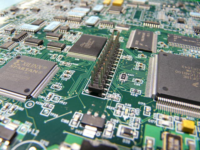
HDI technology gives designers more space on their PCBs to place smaller components even closer together
Due to the growing complexity of design structures, high-density circuit boards (HDI) are being used more and more. As products increase in functionality and decrease in size and weight, circuit board engineers need new solutions to maximize space on each board. Blind and buried vias and vias-in-pad add complexity to the design, but let you do more with less. Royal Circuits focuses on these advanced technologies.
Types of HDI PCBs include:
- through vias from surface to surface
- buried vias with through vias
- two or more HDI layers with through vias
- and passive substrate with no electrical connection
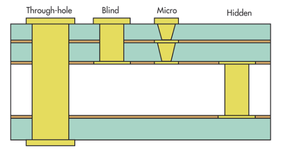
PCB vias come in different configurations:
- Through-hole (TH) vias originate and terminate at the outer layers of the PCB
- Blind vias originate on an outer layer and terminate on an inner layer
- Buried vias are completely buried within the board, connecting only inner layers and not reaching the outer layers at all
- Microvias are a form of blind vias that penetrate only one or two layers, and they have an extremely small drill hole
Below are a few images that illustrate different types of vias
Vias come in different configurations including through-hole, blind, micro, and hidden.
Multilayer boards can incorporate different types of vias to minimize the number of layers required.
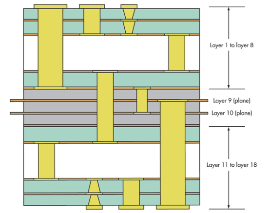
Images from Electronic Design, “Use Advanced PCB Technology To Produce 50% Smaller Product Designs.”
Additional HDI and UHDI Resources

Herb Snogren to Lead Entry into Ultra-HDI Technology
Mr. Snogren Brings Over 40 Years of Experience and Industry Insights to the Company Herb Snogren ...

High Speed Material & Technology for Flex PCBs
In this webinar, learn how to select the right materials and technology for your high-speed ...
High Speed Materials
When your signal frequency approaches 10 GHz, copper roughness and fiberglass smoothness and quality come ...
High Speed Designs
With rise times falling in each generation of integrated circuit development, electrical engineers are quickly ...
Summit Interconnect is celebrating 10 years of trusted PCB manufacturing and the partnerships that have made it possible.
Explore Our Story