Your connection to advanced PCB manufacturing

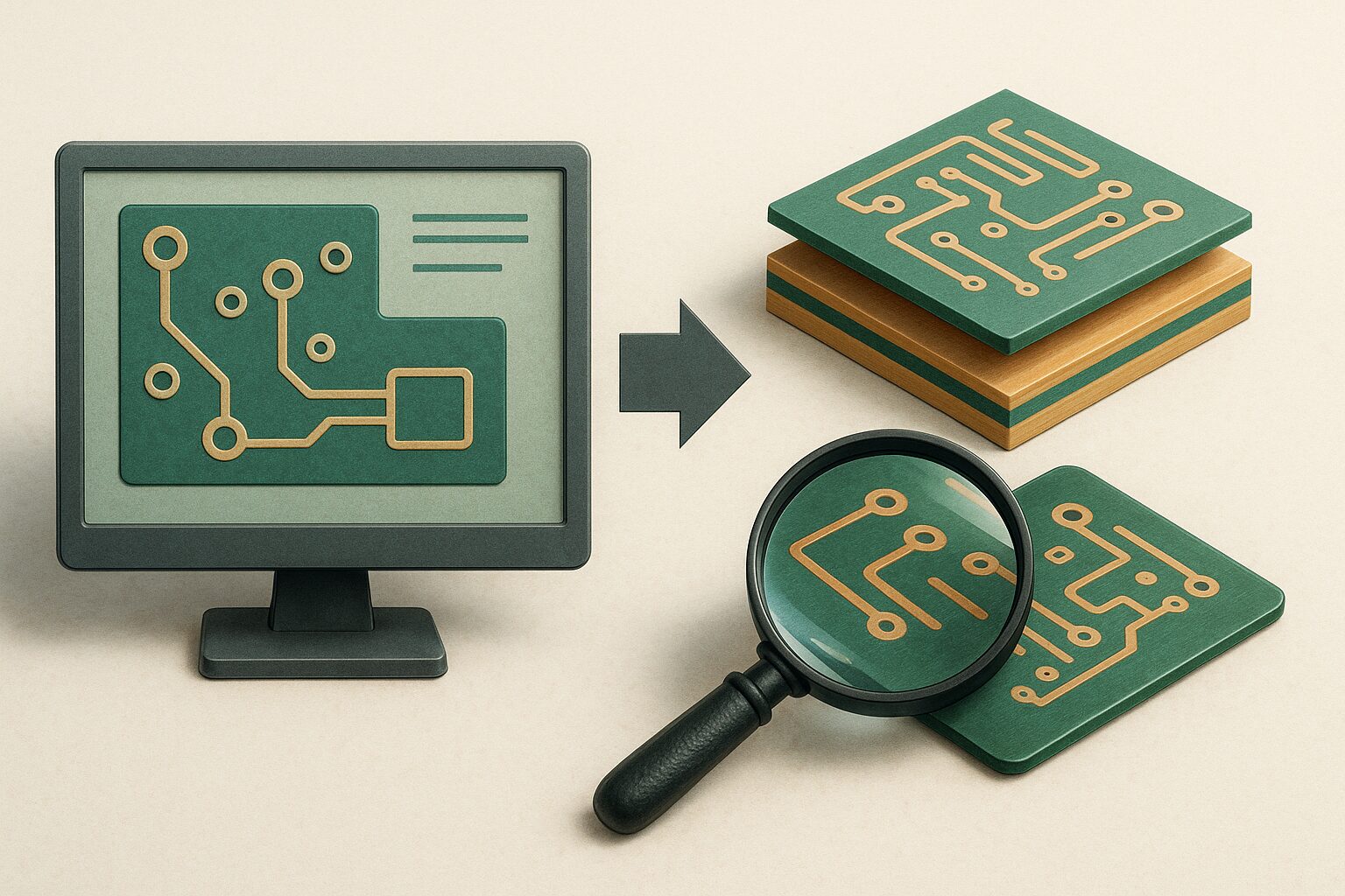
RF and microwave PCBs aren’t just signal carriers—they’re performance enablers. In the GHz realm, every micron matters, every impedance misstep echoes, and every thermal imbalance shortens the product lifecycle. From radar to satellites, high-frequency design is a discipline where precision separates success from noise.
Challenges in RF & Microwave PCB Design
1. Material Selection
Choosing the right substrate material is critical for minimizing signal loss and maintaining impedance stability. Traditional FR-4 materials may not be suitable due to high dielectric loss at microwave frequencies. Consider factors such as:
- Dielectric constant (Dk): Lower values reduce signal delay and distortion.
- Loss tangent: Low loss tangents improve signal transmission.
- Coefficient of thermal expansion (CTE): Compatible materials prevent mechanical stress and misalignment.
Suggested materials include:
- PTFE, Rogers RO4000, RT/duroid, Taconic, or other low-loss laminates
- EM892K, EM890K, EM528, Megtron 7N, Megtron 8, Tachyon 100G, and I-Tera for wider dielectric thickness options that process more conventionally in fabrication
- Low Dk values (2.2–3.5) for signal velocity and impedance consistency
- Low loss tangent (<0.005) to maintain signal amplitude
- Matched CTEs to prevent delamination or misalignment during thermal cycling
Material callouts should comply with IPC-4101, IPC-4202, IPC-4203, and IPC-4562, ensuring compatibility with high-frequency, high-reliability applications.
2. Controlled Impedance, Signal Integrity & Loss Management
RF designers must understand not just what’s on the board—but what’s happening between the layers. RF and microwave signals are highly susceptible to attenuation, reflection, and interference.
- Insertion loss occurs when signal power is lost as it travels through the PCB traces.
- Reflection loss results from impedance mismatches, leading to signal degradation.
- Crosstalk and EMI increase as frequencies rise, requiring effective shielding and grounding techniques.
Best Practices:
- Use controlled impedance transmission lines: microstrip, stripline, and coplanar waveguides
- Maintain tight tolerances in trace width and dielectric thickness
- Avoid right-angle bends; use mitered or curved traces to maintain impedance
- Simulate impedance paths using tools like HFSS, CST, or ADS before finalizing the layout
Impedance control should be verified per IPC-2221 and IPC-2141, with test coupons and acceptance per IPC-TM-650 test methods.
3. Manufacturing Constraints
Unlike standard PCBs, RF and microwave PCBs require:
- Etching and plating tolerances within ±0.001 inch
- Layer-to-layer registration tighter than standard PCB norms
- Specialty lamination and bonding processes to prevent skew and delam
- Smooth copper foil (rolled annealed preferred) to reduce conductor loss
Conformance to IPC-6011 and IPC-6012 ensures acceptable quality levels. Copper foils and surface finishes should follow IPC-4562 and IPC-4552/4556 standards.
4. EMI, Crosstalk, and Isolation
In RF design, proximity breeds interference. Best practices include:
- Ground plane continuity and stitching vias to reduce return path impedance
- RF shields and enclosures to prevent emissions from coupling across zones
- Differential routing for noise immunity where applicable
- Avoiding parallel signal paths that invite crosstalk
EMC considerations and layout techniques should align with IPC-2223. For shielding structures, refer to IPC-4103 for conductive adhesive and metal bonding materials.
5. Thermal Management
High-frequency signals generate heat, which can degrade performance if not managed properly. Metal-backed PCBs, via-in-pad techniques, and thermal vias help dissipate heat and maintain circuit reliability. Strategies include:
- Via-in-pad or thermal via arrays to draw heat into internal layers or backing plates
- Metal-backed PCBs for power-dense designs
- Even copper weight distribution to reduce mechanical stress during reflow
- Implement via stitching to transfer heat away from critical areas.
Plated through-hole thermal reliability should follow IPC-6013 Class 3 requirements. Thermal mitigation via copper balance is discussed in IPC-2221 and IPC-2152 for current/thermal correlation.
Conclusion
Designing RF & microwave PCBs presents unique challenges, but careful material selection, precise impedance control, and proper shielding techniques can significantly enhance performance. By following best practices, engineers can develop high-frequency circuits that offer superior reliability, minimal signal loss, and optimal thermal management, ensuring seamless integration into advanced electronic systems.