Your connection to advanced PCB manufacturing
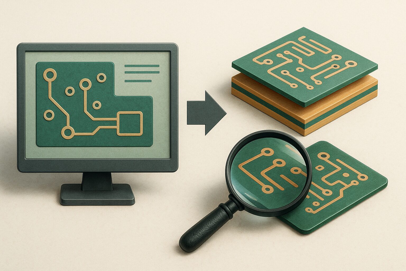
Designers often assume that once their layout is complete and exported, a manufacturer can simply “hit print” and start fabricating boards. In reality, the path from CAD to PCB involves a complex translation of digital intent into physical instructions. Every gap, conflict, or assumption in the data package can slow the process, add cost, or result in boards that don’t match the design intent.
From Design Files to Manufacturing Instructions
A typical data package includes Gerber or ODB++ files, drill charts, stackups, fabrication notes, and sometimes a netlist. The manufacturer imports these into CAM software and prepares the job for the production floor. This is where missing or contradictory details surface such as a drill chart that doesn’t match the stackup; fabrication notes copied from an older design;, or solder mask openings that don’t align with pads.
Each of these discrepancies forces the fabricator to either pause and request clarification or make internal corrections. Both options come at a cost to either your schedule or to the circuit board accuracy.
The Gap Between CAD and Manufacturability
Just because a feature can be drawn in CAD doesn’t mean it can be produced reliably. Fine lines, tight spacing, or aggressive via structures often fall outside proven manufacturing limits. Manufacturability is about yield and repeatability, not just geometry.
Good design-for-manufacturability (DFM) practice accounts for:
- Drill tolerance and plating buildup when specifying pad sizes
- Balanced copper distribution to prevent warping during lamination
- Solder mask clearances that ensure durability during assembly
Designers who consider these realities early create boards that move through production faster, with fewer questions.
The Role of IPC Standards
Industry standards such as IPC-6012 (Qualification and Performance for Rigid PCBs) define the baseline for acceptability — covering annular ring, dielectric spacing, hole wall quality, and more. Aligning with these standards in your documentation reduces ambiguity for manufacturers.
But IPC standards alone aren’t enough. A design can technically “meet spec” while still being extremely difficult to fabricate. That’s why direct communication with the fabricator remains essential.
How Manufacturers “Fix” Your Data
When packages arrive incomplete, manufacturers often make corrections behind the scenes: rebuilding stackups, adjusting drill sizes, realigning solder mask, or cleaning up silkscreen. These fixes take time and can introduce risk if assumptions don’t match the designer’s intent.
Common mistakes include:
- Outdated fabrication notes from prior designs
- Drill charts that don’t align with the Gerber data
- Netlist mismatches that hide missing connections
- Pushing design rules beyond proven process capability
The more manufacturers have to “interpret,” the greater the chance of delays or mismatches.
Collaboration is the Real Time-Saver
The best outcomes come when designers and fabricators work together early. Even a quick DFM review before release can prevent days of back-and-forth later. Sharing preliminary data gives the manufacturer a chance to flag risky design features or clarify material choices before the design is locked.
Best Practices for Strong Data Packages
To minimize risk and accelerate builds, it is recommended that PCB designers provide:
- An accurate fabrication drawing with stackup and drill schedule
- Matching netlist and Gerber/ODB++ data
- Fabrication notes specific to the design (not copy-paste boilerplate)
- Clear impedance requirements and copper weights
- Verified solder mask and silkscreen layers
Always check output files in a viewer before sending them. If you see the board the way you expect it, the manufacturer will too.
Closing Thought
PCB fabrication is more than producing a set of drawings — it’s building a product that must work reliably in the real world. The quality of the data package determines how smoothly that translation happens.
Good PCB design isn’t just about getting circuits to work in CAD. It’s about communicating intent clearly, so the manufacturer can build the board right the first time.
Summit Interconnect has two types of DFM reports to help create a reliable and cost-effective design. These reports help eliminate potential holds and get PCBs in your hands without unnecessary delays. Read more about our technical support and DFM services.