 Your connection to advanced PCB manufacturing

Present-day printed circuit boards contain a plethora of critical components, yet nothing is more vital for efficiency than the surface itself. The surface of modern PCBs performs two main functions: providing a solderable surface to strongly attach electrical components to and protecting exposed copper circuity by using the right finish.
Within the PCB assembly and manufacturing process, a surface finish is the ultimate key to enhancing the durability and longevity of a completed circuit board. This vital coating lies between a component and the bare board. Let’s examine closer the most standard finishes for PCB assemblies. Here are five different types of printed circuit board surface finishes to keep in mind for your project.
Hot Air Solder Leveling: HASL
HASL is a common surface finishing option—the tried-and-true method for a wide array of PCB projects. This is because HASL is a finish type that’s widely available and economical for long-term use. HASL works well for through-hole component boards as well as circuit boards with larger SMT components. Essentially, the protective coating forms after submersion into molten solder and leveling with a hot air knife. This well-known finish is not ideal for fine-pitch, sensitive handling, or smaller intricate surface mount component due to leveling inconsistencies. If lead is a material concern, lead-free HASL is also an alternative with an excellent shelf-life that meets RoHS regulations.
Immersion Silver or Immersion Tin
Immersion coatings are far better options for board surfaces containing smaller components. IAg is a non-electrolytic silver immersion finish that forms via a chemical process. The silver surface layers typically diffuse the copper layer through an immersion reaction. Stable and suitable for fine pitch, this reliable method also provides quick signal speed. It is important to keep storage conditions in mind, as silver tends to tarnish through air exposure.
On the other hand, immersion tin is a cost-effective alternative finish that is RoHS compliant. Similarly, the flat coating is ideal for smaller components, fine pitch, and faster circuitry speeds. However, if your production volume isn’t high, you may desire to stick with immersion silver to avoid ISN’s drawbacks.
Organic Solderability Preservative: OSP
OSP is a simple coating process that works wonderfully to ensure flat surfaces. The thin water-based finish consists of organic carbon compounds that protect the copper for sturdy soldering. While OSP eliminates the need for metal surface finishes, the RoHS-compliant material is not as commonly used today.
Electroless Nickle Immersion Gold: ENIG
ENIG is the most utilized lead-free coating of these five different types of printed circuit board surface finishes. ENIG is a two-layer metallic surface coating—nickel as the main barrier layer for soldering—and gold as a thin protective layer over the nickel. Since the plating is incredibly durable and sturdy, users can expect a longer shelf life. However, the more complex process does raise finishing costs.
Uncertain of what surface finish you will need for your PCBA project? Consult with a professional for a cost-effective design that ensures optimal performance. You can turn to Advanced Assembly for quick-and-easy printed circuit board turnkey services. The highest-quality results await—contact us for a quote today.
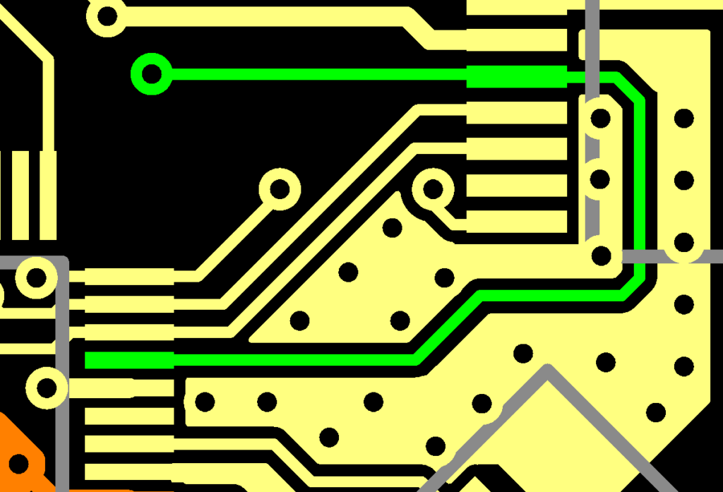
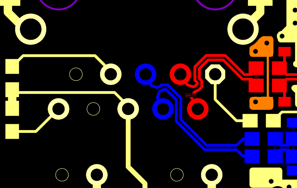
When it comes to creating printed circuit boards, engineers often guestimate various aspects of their design. One such design metric is known colloquially as Trace and Space. Trace refers to the width of a particular copper track, and Space refers to the width of the gap between two adjacent pieces of copper.
The trace and space are based on a variety of factors. This post provides basic instructions on how to determine appropriate trace and space guidelines.
Impedance Control
RF Engineers and High-Speed Digital Design engineers have to carefully route their traces (and their signal return paths) through the various layers of their boards. Dr. Eric Bogatin often states, “There are two types of Antenna Engineers: Those who know they are designing antennas, and those who don’t.” So, to keep the reflections and radiated emissions of your board low, you need a constant impedance on high-speed digital and rf nets.
Whenever a copper trace changes width, layer, or substrate, the speed of propagation changes and a portion of the signal is reflected or radiated into space. It is important that differential-pairs and single-ended high-speed digital signals are given route priority at the very beginning of your design to minimize layer transitions and traces from other nets should not cross above or below these lines unless there is a plane-layer between them.
Once you know you have an impedance-controlled trace on your design, you should communicate with your fabricator, who will determine the trace and space specifications you can use to route your design. The fabricators combine simulation software with real-world experience to determine the proper specifications.
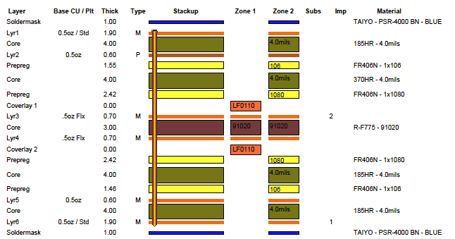
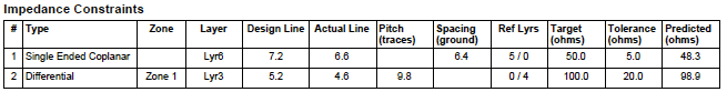
Each layer of your design has unique material properties and can potentially require different trace and space requirements to achieve a constant impedance. If you have a 7 mil-trace with 14-mil space on an external-layer, there is very little chance that those same numbers apply to the net when you transition to an internal layer.
Temperature Control
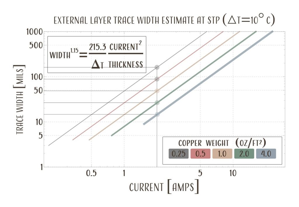
Power-design engineers are usually more concerned with their board bursting into flames than with their eye-diagrams closing. So, the question they usually ask is “How much current can I put through this trace?”. That answer was originally given in IPC-2221, which has been updated by IPC-2152.
IPC-2152 was released five years ago and should be used for estimates only. All prototypes should be field-tested before going into mass-production. Below is an updated graph to be used for estimates only.
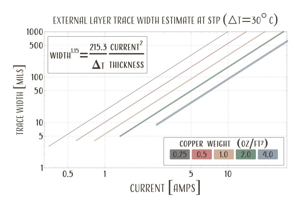
To use the graph package, determine the maximum safe operating temperature for your PCB substrate, as well as the maximum expected environmental conditions of the design as well as an appropriate derating factor. Maximums are not the only consideration. The stresses caused by mis-matched coefficients of thermal-expansion play a role as well. Thermal cycling at relatively low temperatures might destroy your design long before you ever approach an upper temperature limit.
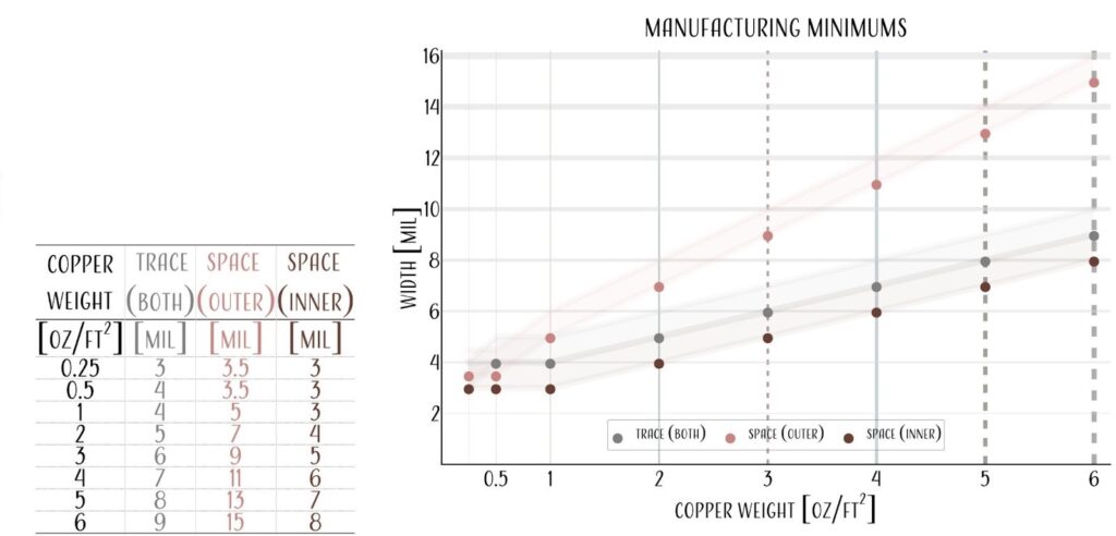
Manufacturing Minimums
Whenever a design pushes the absolute limits of manufacturing, not every board on a panel will work. The ratio of successes to tries is known as the “yield” and controlling the yield is critical to keep the cost of your design low. So, whenever you talk to a fabrication-house, and ask them what their absolute minimum trace/space guidelines are, you should also ask them what their “preferred” minimums are as well.
Conclusion
These are just three factors that affect your trace and space guidelines for ridgid circuit boards. Remember though, they are only guidelines. Engineers are ultimately responsible for the designs that they make. Make sure you give yourself time to test your device in the field.