 Your connection to advanced PCB manufacturing

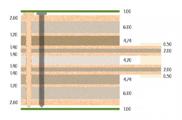
What is a Stackup?
PCBs are made of alternating layers of conductors and insulators (dielectrics).
Multi-layer PCBs are either made by laminating two or more premade cores together, or by starting with a core and laminating foil on the outside to build up the outer layers.
The conductor for rigid PCBs is almost always copper. Occasionally you will hear about aluminum in the middle of the board, but it usually is there to act as a thermal conductor, not an electrical conductor. The insulators are made of a variety of materials that range from inexpensive and easy to work with fiberglass to expensive and hard-to-fabricate Teflon (for RF designs.)
The copper layers are counted from the top to the bottom and referred to by their layer number: “Layer 1”, “Layer 2”, etc… Often, you’ll hear the layers referred to as other things, including “inner-layer”, “outer-layers”, “plane-layer”, “signal-layer”, “top-layer”, “bottom-layer”.
Symmetry
A general rule for designing a core stack is to ensure that it is symmetrical about the middle.
If your stack is not symmetric, differential coefficients of thermal expansion will likely cause the board to warp during assembly and operation. This is primarily a problem on very thin PCBs. Copper acts to constrain the expansion in places & directions where it is present but does very little to constrain expansion in lateral directions.
This type of warpage is caused by uneven copper etching on opposite sides of a core.
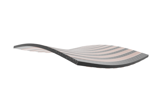
Most engineers know that they need to design a balanced layer stack to prevent warpage during assembly. But it’s pretty often the case that engineers will remove large amounts of copper during the routing process resulting in an unbalanced stackup. If you don’t keep track of your copper symmetry, you will end up designing a potato chip.
What designers should know about maintaining minimum annular ring requirements. This post will share, from a fabricator’s perspective, best practices to achieve first revision success in regards to IPC-6012 requirements and IPC-2221 design guidelines.
Background:
This post is to help PCB designers to understand how the actual drill diameter differs from the fabrication drawing specified finished hole size, and the impact on required annular to fabricate a compliant printed board. This post will also share best practices for documenting vias and component plated holes that clearly indicates finished requirements while allowing the printed fabricator the highest latitude to achieve compliance with the highest possible yield.
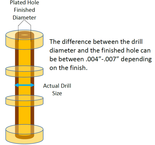
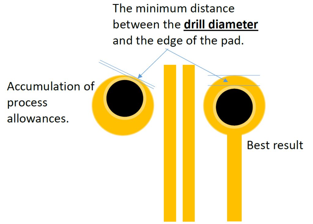
First the basics, “what is annular ring”? Annular ring is defined differently between outer layers and inner layers. For outer layers the minimum annular ring is the minimum distance from the inside side of a finished plated hole to the shortest distance on the outer layer land.
Inner layer annular ring is based on the drill diameter and the shortest distance to the edge of the drilled land. Finished holes size is not considered.
Now that we have reviewed the observable differences between outer and inner annular rings let’s review the IPC-6012 revision E table 3-9.
Class 3 External layer minimum allowed annular ring is .001969” measured from the inner diameter of the finished plated hole to the shortest edge of the plated land.
Class 3 Internal layer minimum allowed annular ring is .000975” and is measured from the drill diameter to the shortest distance to the edge of the land.
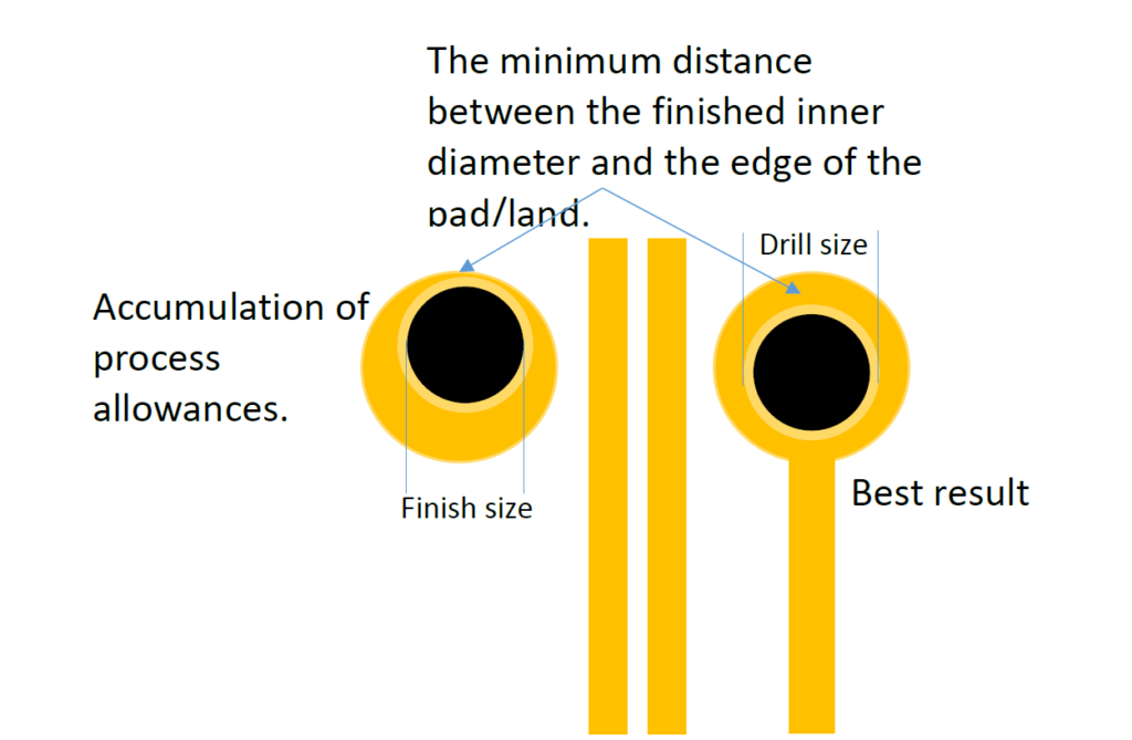
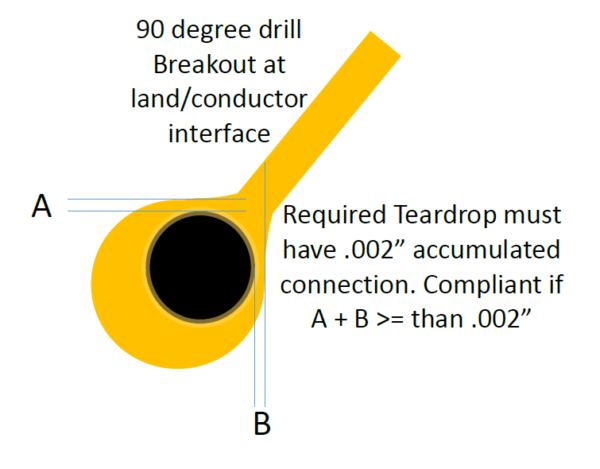
Class 2 allows for 90 degree breakout as long as there is a teardrop/filleting/keyholing at the land conductor junction. Here is an illustration to help explain what is allowed and what is required.
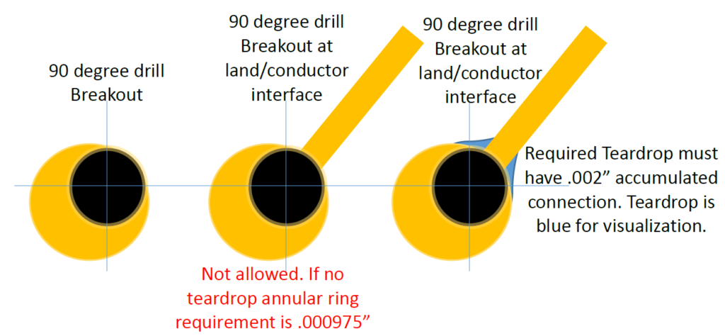
With increased densities many class 3 designs can’t achieve a minimum .000975” minimum annular but can’t accept 90 degree breakouts for high reliability. A useful comprise is the allowance of tangency as long as teardrops are added to the land/conductor interface.
Several of my customers affectionately call Tangency “Class 3 light”. At this time this condition is not classified for mechanical plated holes in IPC-6012 or IPC-A-600. If you choose this option in your design you will need to make a specific note for this allowance. This condition is known as an AABUS condition (As Agreed Between User Supplier).
The second part of this post is to help designers determine how much annular ring is required. This value will depend on the complexity of the design. I would recommend that designers review IPC-2221 section 9.1.1 and all of 9.1.2 and table 9-1.
As a designer if you have ever had a fabricator call and inform you that the design does not have enough annular ring for compliance, this section will help you to understand why the fabricator requires adequate annular ring when it would appear that there is enough currently in the design.
To start off registration of a drill and the lands on all the layers are not a perfect process. Here is a simple breakdown of processing tolerances and why they exist.
- Material, epoxy woven material that we purchase varies in a lot and from one purchased lot to the next. This variation is typically about +/-.0002” per inch. If you take this value across the working area of a production panel. You will find a variation range at .0025” on each side of a production panel.
- Front to back registration of a modern Laser Direct Imaging system is typically .001”.
- Post etch punching of an etched core accuracy is .001” at best.
- Lamination pinning and tooling adds another .001” of tolerance.
- IPC-2221 table 9-1 provides guidance to increase the annular ring .001” if the layer count is greater than 8.
- Drill machine zero position and drill run accuracy can add .001” of increased tolerance range.
- Drill bits can wander. The top layer drilled is accurate, but all drill wandering will impact the lower layers in the stackup.
- Multiple sub lamination constructions will add an additional .002” of tolerance when multiple sub-lamination structures are laminated into the final assembly.
Please note the following values are based on the actual drill bit diameter NOT THE FINISHED hole size.
When we look at the accumulated process values we will did divide the tolerance in half. This can be halved since we split the error across the production panels. So if we add everything together for a high layer count single lamination cycle the process allowance can be .0045” for tangency. If the job has multiple lamination cycles the allowance for tangency would be .006” for the final drill.
If you’re considering Class 3 than the annular ring value would increase an additional .001” so for a single lamination cycle we typically ask for a .006” annular ring. For multiple lamination cycles we will allow a .006” annular on the first sub-lamination cycle but will ask for .007” annular ring on the following lamination cycles.
The last item for designers to consider is what drill size does the fabricator actually drill width. To answer this question it would be beneficial if the designer has two rules. One for plated vias in which finished hole size does not matter, and two component holes sizes that typically has a lead in finished plated hole. Component holes should list the finished hole size and the allowed tolerance.
Vias should be stated as vias and that the finished hole size may finish to any size less than the specified drill size. Most designs list the via size that matches the actual drill bit size the fabricator should use. Using the actual drill bit size will provide the correct annular ring and a “safe” keep back distance between a drill bit and a different net. To clearly convey that a particular drill is a via, the designer should use the following tolerance in the drill chart. This examples uses a .010” via size.
Drill X .010” +.002”/- drill diameter.
This instruction makes it clear, to the fabricator, that the designer implies that the design has been configured and checked with a .010” drill bit. A fabricator can look at this requirement and make a determination which drill bit will provide the best yields as long as the finished hole is .012” or less. In some cases a fabricator will drill larger if there is plenty of annular ring, or they may elect to drill smaller to ensure that the finished part will have compliant annular rings.
Component holes. These values can vary between fabricators. For component holes, a fabricator must compensate the drill size for plating and variations of the hole size after all fabrication processes have been complete. Here are typical value and these values should be considered during the DRC checks in CAD.
Immersion finishes ENIG, ENEPIG or Silver the drill size is .004” bigger than the finished hole size.
Hot Air solder level (HASL) finish the drill will be .006” larger than the finished hole size. HASL cools down in an ununiformed manner and closes down the finished hole size.
Tin Lead plate reflow may be drilled .007” larger than the finished hole size. During the reflow process this can close down the hole more than HASL.
If a higher hole plating thickness is required it will be necessary to increase the manufacturing drill bit diameter to meet the additional plating requirement.
Summary:
I hope this information will be beneficial to help provide your future designs with no issues that otherwise would be caught at the fabricator. My intent on these post is to help designers to achieve error free designs that go from your CAD system thru our CAM systems with no DRC findings.
And just for the record, this post is based on managing a Fabricator’s engineering department for 20+ years and nearly 40k different designs. Summit Interconnect builds advance R&D products with .004” diameter drill in .0097” lands and Class 3 mil/aero and space products.
Well that’s it in a nutshell. Your questions and/or suggestions are welcome.
Stay healthy and safe everyone!
Gerry Partida