 Your connection to advanced PCB manufacturing

Whenever you route a signal trace, you need to pay attention to the return path for that trace — return signals take the path of least impedance, not the path of least resistance. Ideally, every digital signal line and power rail will have an uninterrupted return path on an adjacent layer. But board layers do not have even spacing, and many designers forget about this fact, especially at the beginning of their career.
If, for example, you choose to have ground on layer 3 and signal on layer 4, the return path is close, and the field lines will be contained to layers 3 and 4. But, that’s horrible coupling for layers 1 and 2, as they are too far away. Signals on layer 1 will have no choice but to either attempt to pass through layer 2 (which they won’t likely do) or they will simply find a new return path through your power plane, increasing your power rail noise. The power-plane will be far from the ground plane, so the field lines will have ample room to spread and create unwanted noise, and there will be little benefit from capacitive coupling.
A better 4-layer layout has ground on layers 2 and 3 and mixed power/signal on layers 1 and 4. There, the short distance will ensure that the signals are tightly confined to their return paths.
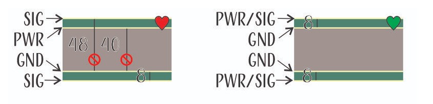
All of that said — as a beginning designer, you should stick to the first, lest preferred option. You’ll have plenty to deal with routing your first project without having to worry about Signal and Power Integrity. Our first design can be made on a solderless breadboard — with the exception of a few components, layout isn’t terribly critical.
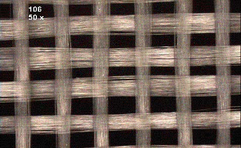
The simplest common stack up consists of two layers of copper separated by a fiberglass/epoxy core. The fiberglass provides strength and rigidity and the epoxy provides an adhesive force that bonds the fiberglass to the copper. Other materials, such as Teflon and polyimide, are available but are often outside the price range of most projects, so they are not discussed here.
The fiberglass layers range in thickness from <1 mil to >50 mils thick (made by stacking thinner layers of fiberglass) and provide mechanical strength and dielectric medium for the surrounding copper layers.
It takes time to attach copper layers to one another, so to move quickly, most PCB manufacturers have a stockroom full of an assortment of prefabricated two-layer FR-4 stacks in common copper weights and core-thicknesses. You can save time and money by selecting a core that your manufacturer commonly stocks.
Prepregs
“Prepreg” is short for “pre-impregnated.” Prepreg is a thermally activated epoxy that is used to bond two layers of copper or core material together. Often the copper has been etched at this point, so there are height variations of 1-6 mils between the top and bottom of copper foil. To prevent cavities, (or measling), fabricators have to use a material that has a lot of epoxy, which doesn’t allow for a tight fiberglass weave like in the core material.
Epoxy
The epoxy is mixed with the fiberglass to create the prepregs. It is activated at specific temperatures under carefully controlled pressures. Excess epoxy is forced out of the side of a panel during assembly. Your fabricator will select prepregs with specific resin contents for your design, based on a variety of factors, including the thickness of adjacent copper layers.
Considerations
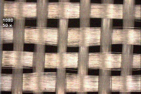
Fiberglass and Epoxy have different material properties and different dielectric constants. Most Dk values presented in datasheets are an average of the Dk of the epoxy and the Dk of the fiberglass. But your traces will experience a slight change in impedance as they travel over each warp and weft yarn in a board. For impedance controlled traces, your best bet is to use a “flat-glass” or “e-glass” core material that has a tight fiberglass weave and a low amount of epoxy and ensure your traces are coupled to the copper on the other side of the core.
Construction
To make a four-layer board, your manufacturer would:
- Start with two pieces of two-layer copper-clad core material, place prepreg between the cores, or
- Start with a core, place prepreg and copper foil on either side.
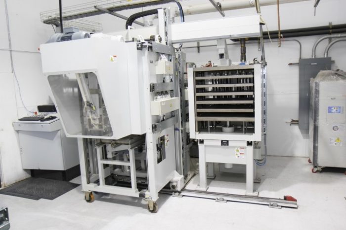
Then the stack would be placed in a hot-oil hydraulic press for several hours.
Any number of core layers can be attached during a lamination-cycle. However, if even one of the layers shifts a bit too much during the process, the entire panel will have to be thrown out.
To save money on your design, try to use common core sizes and limit the number of lamination cycles. You can communicate directly with your fabrication house to decide on the layer stack early in the design process.