 Your connection to advanced PCB manufacturing

Every Electronic Design Automation (EDA) tool is a bit different. Some have more features than others, some have different features, some offer simulation, some don’t. But they all have a few features in common: they allow designers to capture a schematic and layout a PCB.
In a schematic diagram, components are represented as abstract symbols.
On a printed circuit board, components are attached to copper pads arranged in carefully designed land patterns.
To create a design, you need a part library that has all of your components’ land patterns associated with the components’ schematic representation.
Basic EDA Structure
There are four basic parts of every EDA tool. The pattern editor, component editor, schematic layout, and PCB layout program. The names of the modules might vary from program to program, and they might be used differently, but they all exist in one form or another.
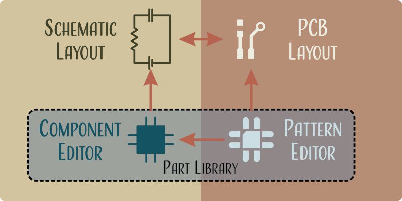
- Component editors alter the appearance of schematic symbols.
- Pattern editors alter the appearance of land patterns.
- Libraries hold collections of linked components and patterns for reuse from design to design.
- Schematic Layout arranges the connections between components.
- PCB Layout arranges the patterns and the traces that connect them.
Libraries hold groups of footprints and components. When a component is selected for use in a schematic, it’s associated land pattern is prepared for use in the PCB layout portion of the software.
Pattern Editor
Engineers use the term footprint to describe the outline of the bottom of a discrete component and its pads/pins.
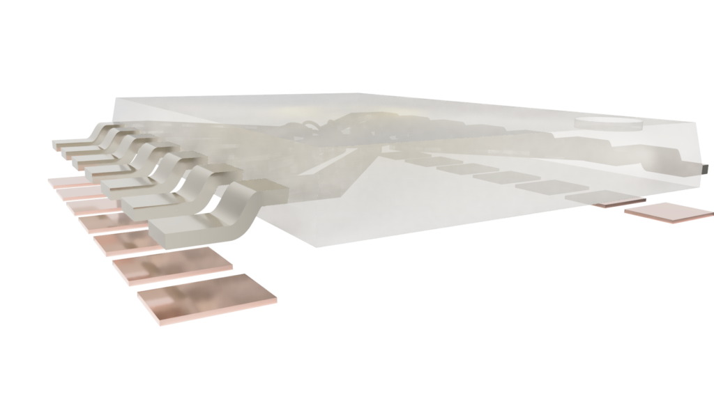
To make things even more exciting/confusing, the land patterns associated with those pads are often incorrectly called footprints by engineers, even though the metalized lands have to be larger than the metalized pads/pins they mate with.
Discrete components have metalized pads or pins on their base and sides.
Printed circuit boards have metalized lands on their outer layers.
These two metalized parts have a similar pattern but are two different sizes. Solder connects the lands to the pads/pins.

For a proper solder joint to form, the solder has to form a filet, and the only way that can happen is if the land is bigger than the pad/pin.
A discrete component’s metalized pad pattern and a printed circuit board’s land pattern are identical in layout and centerline spacing, but the metalized lands are always bigger than the metalized pads.
The size and shape of footprints and lands has been largely standardized into IPC-7351, a document that describes the pin pattern, layout, and naming convention for all standard parts.
Component Editor
The abstract symbols that represent PCB components are created and edited in a component editor. Components are shapes that abstractly define the function of a physical part, with pins that represent metalized pads/pins on physical components. There are two standards in broad use and as long as the symbols don’t jump from one standard to another within a schematic document, it’s usually pretty easy to keep track of what is going on.

Schematic Capture
Schematic Capture is the part of the program that takes the components from the library and lays them out on a document. Parts are connected with virtual wires that allow designers to see the electrical connections between pins. A set of pins that are electrically connected is called a net.

When you pull a component from the library, you should do two things.
Make sure the part is available. It’s very common for EDA part libraries to be out of date and include parts that are now obsolete and unobtainable.
Double-check the land pattern that is associated with the part number is correct. You never know who made the library entry, and it’s possible that they read the datasheet incorrectly or they copied the footprint in a 1:1 manner.
You should go through a careful schematic review process before you move on to layout. Even the simplest schematic is complicated. Errors caught at the schematic stage can save hours of rework at the layout stage.
PCB Layout
While you have been layout out your schematic, your EDA has been quietly been keeping track of your land patterns, and the connections between the pins. If it’s been set up properly, there’s a good chance that it knows which pins require special routing rules as well.
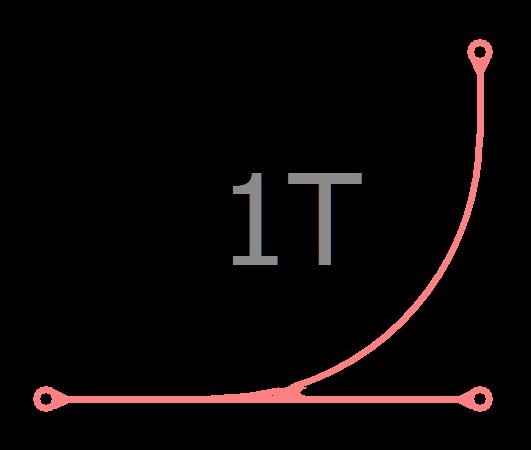
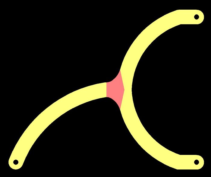
After part placement, the next step is to route traces between nets. An image below shows several examples of traces meeting at a t-intersection.
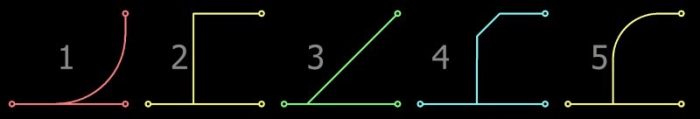
Acid Traps
If you talk to a collection of ten electrical engineers, nine of them will immediately discount options 1 and 3 due to the acute-angle intersections on the right side of where the traces meet. They will tell you that those angles create “acid-traps” — or locations where over-etching can occur. And while that might have still been a problem thirty years ago, fabrications processes have advanced to the state where it simply doesn’t matter anymore. You can draw a 1°-separation between traces on your fab designs if you wish. You won’t have issues with acid-traps, but you will have issues violating fabrication space-width minimums.
If you create a design that has a small angle in it, you fabricator might place a hold on your design. While they can easily close it by editing the gerber files, they have no way of knowing if your decision was an intentional feature to be kept or an oversight to be ignored. And they won’t make your board before checking with you first.
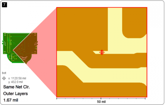
You can check for this problem by enabling “Same-net Clearance” checks while you perform your Design Rule Check in your EDA program.
High-Speed Reflections
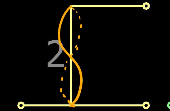
Engineers have a deep-seated hatred for right-angle turns, as shown in example 2 in image 1. A high-speed signal traveling along a trace will see an impedance discontinuity at a right-angle turn and another at the intersection.
Impedance discontinuities can cause reflections — if you have the right frequency and the right trace length, and a bit of bad luck, you can establish a standing wave in your trace. This has happened to electrical engineers, but it’s only a factor in extremely high-speed designs (>10 GHz) and unless your design requires non-fiberglass dielectrics, you don’t really need to worry about it.
The theoretical change in impedance at a right angle turn is 15%-20%. But the actual change in impedance is very difficult to measure.
But the theory doesn’t agree with empirical testing. Voltage transitions are not instantaneous — they occur over some amount of time and over some distance. Even a sub-nanosecond signal transition will occur over 100 – 500 mils distance. Most signal traces are less than ~10 mils wide, which places the discontinuity in that range as well. In short, the discontinuity is so short that it does not substantially affect the signal.
To visualize the discontinuity at a 90-degree bend requires high-end test equipment (oscilloscope with ps resolution and a time-domain reflectometer with ~30×10-12 s rise-time). Most logic-transitions are in the 10-9 or slower range. Therefore, the 90-degree bend simply doesn’t matter in practice.
You only need to worry about right-angles on very, very high-speed designs. There are other ESD and EMC concerns related to right-angles, but they aren’t usually a problem for new designers.
Thermal Dissipation
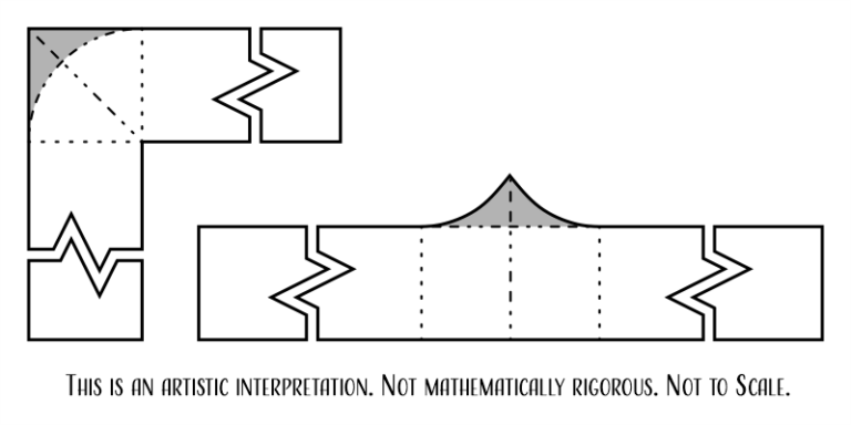
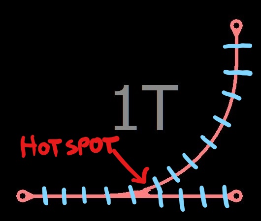
If you have a high-current trace, heat will dissipate outwards from the trace to cooler parts of the board. Usually, the thermal gradient is oriented perpendicular to the trace, outwards in both directions. But what if one of the areas the heat has to dissipate is shared by another part of the trace? Heat does not flow into hot locations — the thermal energy will remain in that section of the board, creating a hot-spot.
Best Option For Your Design
Use Image1, example 4 for your design: Curved traces often take more time to route and are overkill unless you want to use them for stylistic reasons.