 Your connection to advanced PCB manufacturing
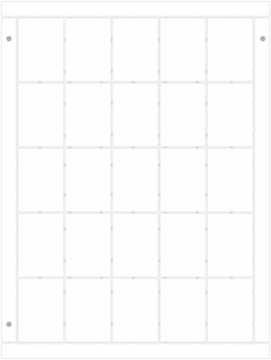
The majority of printed circuit boards made today are produced in batches on standardized panels. If you are trying to minimize the cost of your next design, you should consider your board shape and size.
While some manufacturers will make one-off boards, all manufacturers can make panels that are nominally 18” x 24”, with either a 0.5” or 1.0” margin that is used for fixtures, fiducials, and test coupons. That leaves 16” x 22” (or 17” x 23”) of board space for your next design.
But before you start designing, you need to keep a few things in mind.
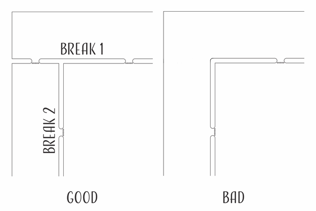
Depanelization
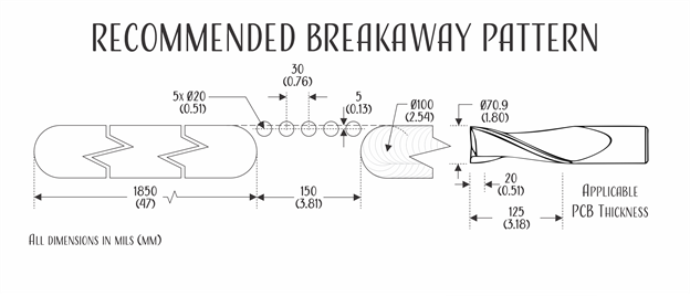
To individualize your boards from the panel, there are two general options in wide use. The first is routing, and the second is scoring. Routing leaves tiny mouse-bites in the board, and scoring cuts a 30-60° path through ⅔ of your board. Laser depanelization is available but is expensive and not discussed here.
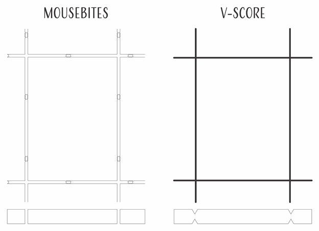
You can have your fabricator create your panel for you (preferred). Or you can create the patterns yourself. Something to keep in mind is that the end-mills used in routers only cut well in one direction, so for clean boards, you’ll need a route-path that is wider than your fabricator’s end-mill diameter.
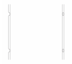
You can use single or double-sided mousebite patterns on your designs to remove the tabs on both sides of the breakaway point.
Avoid Spontaneous Depanelization and Destructive Depanelization
Something to keep in mind whether you use mouse-bites or v-scores is that the boards need to stay in the panel until it is time to remove them. If you make your boards too weak, they can spontaneously disassembly during shipping.
One way to achieve this is with skip-scoring or carefully designed routing patterns. If you create a design that stays strong until the board margins are broken away, you’ll be in great shape.
Straight Line Breaks
Your assembly house should only ever break in straight lines. Doing anything else can put a great deal of stress on your board — something that can damage the laminates and cause your parts to pop off the board.
If you have any further questions, contact our engineering experts for more information.
Build a better via stack by thinking about how your board is assembled.
Cap vs. Foil Construction
Printed Wiring Boards are constructed in one of two ways described as “Cap” or “Foil” construction. The construction method determines via layer options and lamination cycles.
Foil Construction
In foil construction, fabricators start by drilling, electroplating, and etching a copper-clad core that will become the innermost layer of the design. Then additional layers of prepreg and copper are laminated to the outside of that core, and the new layers are drilled, electroplated, and etched. The process repeats until all layers of the board have been added, usually maxing out at 18-24 layers. After the last lamination, the board will be drilled, electroplated, and etched to create through-hole vias.
Very high layer count boards, such as a 96-layer board used for a new microcontroller validation, can be created by combining smaller layer stacks.
Microvias might be added to connect layers 1 and 2 or layers 3 and 4. To connect layers 1 and 3, a designer might create a through-hole via from layers 2 to 3 and then add a staggered microvia from layer 1 to 2. A through-hole via can be added after all layers are laminated.
Cap Construction
In Cap Construction, multiple copper-clad cores are drilled, electroplated, etched, and then laminated. If no blind or buried vias are needed to connect the cores, multiple cores can be joined in a single lamination cycle.
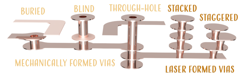
What does it take to make a via?
Mechanical Vias
After multiple layers of copper and dielectric material have been laminated in a hot-oil press, a high-precision drill pierces the complete-assembly or the sub-assembly in all the locations that will eventually become mechanical vias. Next, the panel is placed in a dry-film laminator and a negative-image of the layer artwork is projected on the film, curing it and causing it to adhere to the copper underneath. Then the uncured dry film is removed, leaving exposed copper in all areas that will eventually become traces, copper pours, and vias. The panel then enters an electroplating bath, where copper fills in the via barrels and thickens all exposed copper. Finally, the entire board is etched, which removes all of the unplated copper, and a small amount of the plated copper.
All mechanical (buried, blind, and through-hole) vias are formed in this manner. Buried and blind vias only take their names after additional lamination cycles.
Microvias
Microvias are usually created to join one layer to the next in a foil-construction. Under certain circumstances, a microvia can span two layers, but typically, the microvias would be built up one layer at a time in either a stacked or a staggered assembly.
Microvia holes are created with lasers that pierce through the topmost layer of copper and the underlying dielectric material. The combined thickness of the dielectric and copper is equal to the minimum allowable via diameter.
Microvias may be filled in a variety of ways, but electroplated copper is the most common option.
Why do you need to know all of this?
Once you know the basic processes required to make your board, you can determine whether or not the vias that you’ve specified can actually be formed in your PCB. Then you can start saving money in your next design by minimizing the number of lamination and via formation cycles.