 Your connection to advanced PCB manufacturing
Civil Engineers have a saying: “Any idiot can build a bridge that stands. It takes an engineer to make a bridge that can barely stand.” To achieve their goals, Engineers have finite element and lumped element analysis available to them that allows them to simulate all manner of loading and failure analysis. With that safety information in hand, they can make decisions to decrease cost. The technical aspects are specific to the field of Civil Engineering, but the processes are universal to all disciplines – make it work, make it safe, and then make it inexpensive. Engineering is at its heart, a compromise between competing requirements and risk, with cost and safety usually winning the day.
The same idea can be applied to PCB design. While not every idiot can build a HDI PCB, “It takes an engineer to make an HDI PCB that barely works.” That is because the “barely” can come with significant cost savings. You can absolutely go out and purchase Roger’s core material, use 2 oz. copper, and have a design that works. But can you replace iTera MT40 with 1080 FR4, and the 2 oz. with 1 oz. copper? You will never know until you either simulate your design or take the chance of building your board with less expensive materials. The purpose of this article is to convince your company to invest in the tools you need to do your job so you can purchase less expensive materials from us, and make your overall design less expensive to produce.
The operating frequency of your design isn’t all that important. In your decision to simulate or your selection of test equipment, the critical number
you need to pay attention to is the rise-time / fall time of your fastest signal in your circuit.
It is possible (although unlikely) to have a leisurely 40 kHz switching frequency with a 20 GHz equivalent rise time by using a fast GaN switch. Frequency is the reciprocal of the period, so 1/50 ps = 20 GHz (20 GHz is an approximation since the choice of 80/20 or 90/10 is somewhat arbitrary and I’m ignoring a few other details.) To reiterate — you might be designing a “low-speed” circuit on paper, but in practice, it could be a very, very high-speed design. And those high-speed harmonics, reflections, etc… might completely disrupt your design.
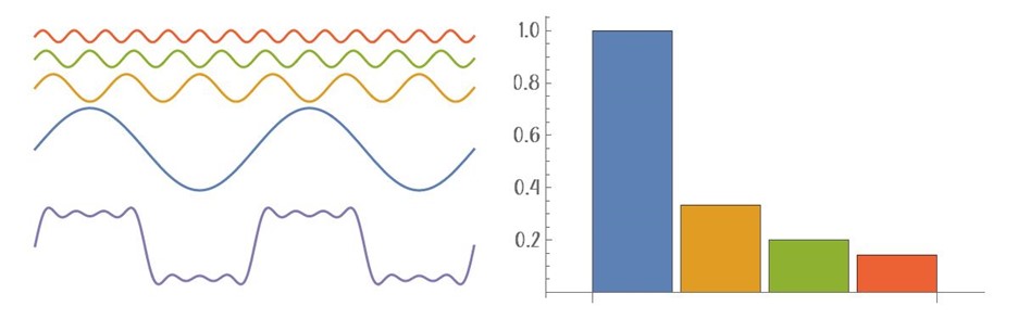
And to make matters worse, it’s not just the fundamental frequency (determined from rise-time) that you need to worry about. In the frequency domain, square waves are made of a series of lower-amplitude, higher-frequency sine waves. And unfortunately, the first few harmonics have sufficient amplitude to disrupt your design as well.
Measurement
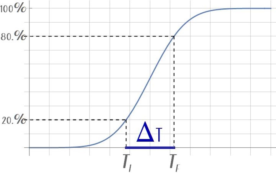
Is your scope able to accurately measure the rise/fall time of your signal? The rise time is usually defined as either the time it takes for the electric potential to rise from 20% to 80% of the maximum value or from 10% to 90% of the maximum value. But most affordable oscilloscopes lack the ability to capture the high-speed signals that modern switching circuits can generate.
As a very quick rule-of-thumb, your scope and probe bandwidth should be at least 60% of the reciprocal of the shortest rise-time interval in your circuit.

For example, a 300 ps signal would require a scope with a 2 GHz bandwidth, and a 1 GHz scope could capture at most a 600 ps signal. Please keep in mind this equation is a “back-of-an-envelope” estimation. To truly determine your needs, you’ll need to know the measurement accuracy required, the frequency response of your scope, the resistance and capacitance of your scope probes, and a few other things. It’s best to just get a test-equipment representative on the phone and explain your requirements and let them tell you which test instruments they have that can meet your needs.
If you don’t have sufficient sampling points, you won’t be able to capture the actual rise and fall times of your signal.
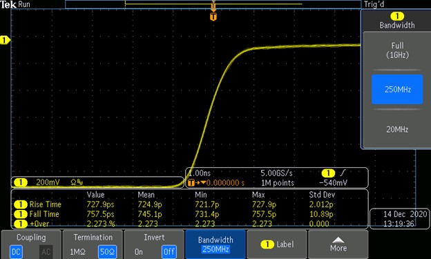
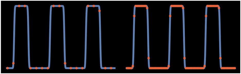
What does that look like in real life? Let’s take a moment to look at some actual sampled signals from a ~40 ps rise-time source on a Tektronix MDO3104 oscilloscope with a rated combined bandwidth of 1 Gsps. The Rule-Of-Thumb provided earlier says that this scope would, at best, be able to see a 600 ps rise time, a difference from the datasheet’s stated rise time by over an order-of-magnitude.
First, set the scope for 250 MHz — as would be the maximum bandwidth on a single channel if all four channels were in use. There we see a signal that’s pretty similar to the first image that appeared in this article. It looks remarkably clean, so you might be tempted to think everything worked out as it should, write down the number, and move on. But be careful.
Now let’s find out what that signal looks like when the entire 1 GHz bandwidth is used and the sampling increases by a factor of four.
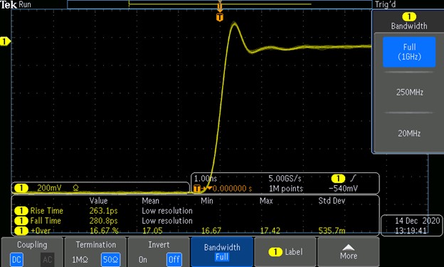
That’s a different signal entirely. And the measured rise time is significantly higher than before as well. We’re not seeing the true rise time of the signal — we’re seeing the limitations of the oscilloscope’s sampling rate.
This image isn’t the true representation of the signal either. Even though we’ve quadrupled the number of sampling points, there still aren’t enough sampled points to accurately capture and reproduce the waveform.
In short — for high speed signals, you need quality test equipment in your lab to truly understand what is happening to the signals in your circuits.
Simulation
Before you ever power on your test equipment or send your artwork to your fab house, you should have a thorough understanding of what is happening in your design. For that you need to find a simulation software suite that fits your requirements and your budget.
Your simulation needs will again depend on the rise-time of your devices. There are a variety of software options out there that fill numerous needs. You need the right tools to do your job.
Etch Progression
Copper foil does not etch right angles to a board surface. Initially, only the exposed copper surfaces react and are washed away by the etchant, largely dissolving material perpendicular to the board surface. Then, as the etchant progresses from the etch resist layer to the substrate layer, there is increased opportunity for lateral material removal. After some time in the etching tanks, liquid etchant removes copper both perpendicular and parallel to the board surface.
At the early stages of the etching process, cross-sections of unprotected copper surfaces appear circular, and then trapezoidal with curved legs, and after extended etching, the sides may appear almost vertical.
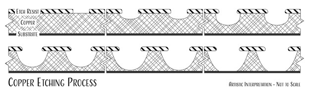
The progression from curved to vertical requires extra time in the etch tanks and the removal of larger-than-normal amounts of copper. Fabricators do not over-etch traces to the point of verticality unless it is specifically requested by a PCB designer.
Copper Etch Compensation
After etching, the copper closest to the etch-resist layer is generally narrower than the copper nearest the substrate layer. To ensure adequate copper width after etching, fabrication houses must adjust copper artwork before fabrication in a process called etch compensation. Based on the copper weight, fabricators will expand copper features into available space by 1-8 mils, so that after etching, the width of the trace meets a specified minimum.
Copper Cut Back and Compensation
Closely packed copper features can interfere with this compensation process. Enough room must exist between copper features to allow the etchant to move freely into an area and copper atoms to move out. To allow adequate etch compensation on critical features, fabricators will sometimes trim the copper away from other nets in a cut-back process.

The Process
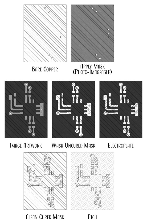
After through-holes are drilled in a panel, copper foil is covered with a photo-imageable etch resist liquid or dry-film mask and then exposed to light in a negative 1:1 pattern of the layer artwork. The light causes chemicals in the mask to polymerize and harden. The unpolymerized mask is washed away and the panel is then attached to the cathode of a pulsed DC power supply and submerged in electroplating tanks where copper accumulates on the exposed copper. The remaining solder mask is then removed from the panel.
At this point the copper foil is thicker in the parts of the board that will eventually be traces, copper pours, etc… In the last step, the entire panel is etched — copper is removed from the entire board. The thinner, un-plated areas of copper etch completely away before the thicker electroplated foil, so after etching, the traces and the copper pours are left behind.
There are a few more details to the process that were not discussed here, such as via fill, electroless catalysts, and more. To learn more, contact Summit’s technology team.