 Your connection to advanced PCB manufacturing
Most engineers know that when an electromagnetic wave encounters an impedance discontinuity at any point as it travels from source to destination, part of the signal energy will reflect, creating noise and dissipating energy as radio waves and heat. But the part they often forget is that the impedance discontinuity needs to be electrically long with respect to the signal transition time before the problem is visible on all but the most advanced test equipment.
It is true that changes in impedance should be avoided wherever possible to prevent reflections and energy dissipation. But very small disturbances, such as the several-ohm decrease in impedance at right-angle corners, usually don’t matter at all.
Car Tire Analogy
Image driving your car along the highway and the driver’s side tires hit a puddle of water. If the puddle of water is only 0.05 mm deep, it’s deep enough to see, but you likely won’t even know it is there, and the change in wheel speed might not be detectable. But if the puddle is 50 cm deep, then the tire on the left side of the car will quickly slow down.
What’s the difference? A car tire’s speed will certainly change when it moves from asphalt to water. But that’s not the only consideration — the depth of the water and the width of the puddle matter too. In the first example, the water’s depth was insignificant compared to the height of the tire and the weight of the car. In the second example, the water depth was more than half the height of the tire.
Back to PCBs
Something similar happens in PCBs. Electrical signals in FR4 materials propagate approximately six inches each nanosecond. Take a look at the rise-time/fall-time in your circuit. If the rise-time/fall-time is 1 nanosecond, then a complete logic transition can take place within a 6-inch trace. The energy from the harmonics in that signal will transition over an even shorter distance. So for a quick rule-of-thumb, assume 1/6th the distance, or 1 inch per nanosecond as the threshold. (This is a little shorter than other rules-of-thumb on this matter, but much easier to remember). Our friends across the pond might use either 2 or 3 cm/ns as the threshold since it is only an estimate.
Here’s what that means: If you have a 1 nanosecond rise time, a minor impedance discontinuity needs to be longer than 1 inch before it will cause measurable signal reflections.
The Myth of Right-Angle Traces for Digital Lines
Right angles on PCBs are such a minor drop in impedance, over such a short distance, that they simply don’t even warrant consideration unless you are designing something with rise-times that are less than 100 ps.
PCB Designers usually give high-voltage and high-speed signals the highest priority of all of their nets — meaning they get routed first, and other signal lines have to route well around them.
If your project runs a low-speed (10 ns rise-time) differential pair a few centimeters between the chip and connector, you don’t really need to worry about high-speed design practices meant for 50 ps rise times.
The first step in any high-speed design happens right after your schematic is finalized and before you route the first trace. Contact your PCB manufacturer and tell them you need trace and space guidelines for a high-speed net.
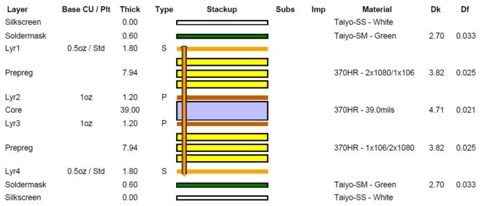
Many free online impedance calculators are not accurate enough because they cannot take into account real-world variables such as squeeze out, epoxy content, and fiberglass weave. PCB fabricators often provide simple stackups to their customers. The stackup engineers will ask several questions, such as what board thickness, copper weight, number of layers, and dielectrics you plan to use. The engineer will then provide you with specific trace and space guidelines using materials that are cost-effective and readily available. Below is an example of a stack up.
The provided trace & space guidelines only work for the layers they are calculated on. If you plan to change layers, you will likely have to change trace and space widths as well. Additionally, when routing your traces, you should not do anything that will change the impedance of your traces such as running them above or below traces on adjacent layers or routing them too close to stitching vias.
Mr. Snogren Brings Over 40 Years of Experience and Industry Insights to the Company
Herb Snogren has joined the company as an industry consultant. Snogren will be leading the latest initiative to add ultra-HDI technology to its existing PCB manufacturing services. He brings extensive industry experience and a strong focus on bringing technological advancements to the US printed circuit board (PCB) market.
Snogren will be responsible for creating new processes and overseeing equipment installations for providing ultra-HDI capabilities. Under his direction, Snogren predicts we will be able to manufacture circuit boards with lines and spaces of 20 to 50 microns in the next 12 months.
“Summit Interconnect has always believed in staying ahead of the curve and offering customers the most cutting-edge manufacturing technologies,” said Milan Shah, president, and co-founder of Royal Circuit Solutions. “Under Herb’s and his brother Matt’s guidance, we will be taking our facility to a whole new level and providing the technology our customers need to create the next generation of innovative, electronic products. I could not be more excited or prouder of this company.”
Snogren began his career in high school where he worked at Reliable Circuit Systems, a printed circuit board factory owned by his father. Together they started SAS Circuits in Colorado.
“Domestically, there are very few PCB fabrication facilities that offer ultra-HDI capabilities and those that do have limited capacity,” said Herb Snogren. “I believe once PCB designers learnSummit interconnect offers ultra-HDI PCBs, they will start designing circuit boards around this capability. Ultra HDI feature sizes allow designers to reduce layer counts, utilize finer pitch components and miniaturize end products.”
Snogren co-chairs the IPC D33AP committee, which is working to develop a global standard for ultra-HDI technology. He is also on the IPC 1791 committee and works with the Department of Defense to ensure it has a robust PCB supply chain.