 Your connection to advanced PCB manufacturing
What designers should know about maintaining minimum safe drill to copper distance and PCB reliability. This post will share why you should follow IPC-2221 Design Guidelines for Print Boards section 10.1.3 for a successful and field reliable Printed Board.
Background:
In the quest to pack more high-speed conductors designers may look for “free” real-estate to achieve this goal. One of these methods, is the removal of Non-functional pads and routing conductors closer to a plated via. This post shares safe practices to ensure that your design activities stays on target for a successful outcome.
The topic of this post is not if PCB inner layer non-functional pads for plated holes should be kept or removed (that is a subject for a future post), but what rules are safe if your design has removed the nonfunctional pads.
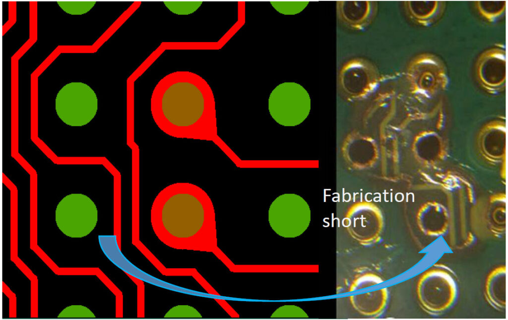
Here is a design with non-functional pads removed and the conductor routed closer to the via. A short occurred in fabrication. In this example the design distance between drill and conductor was .007
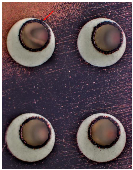
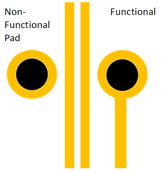
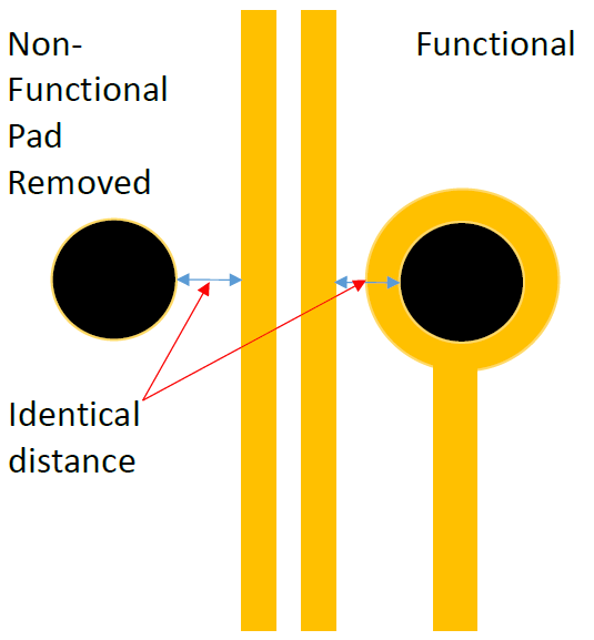
What is a non-functional pad (NFP)? An NFP pad is a drilled inner layer pad that has no connection on a given inner layer.
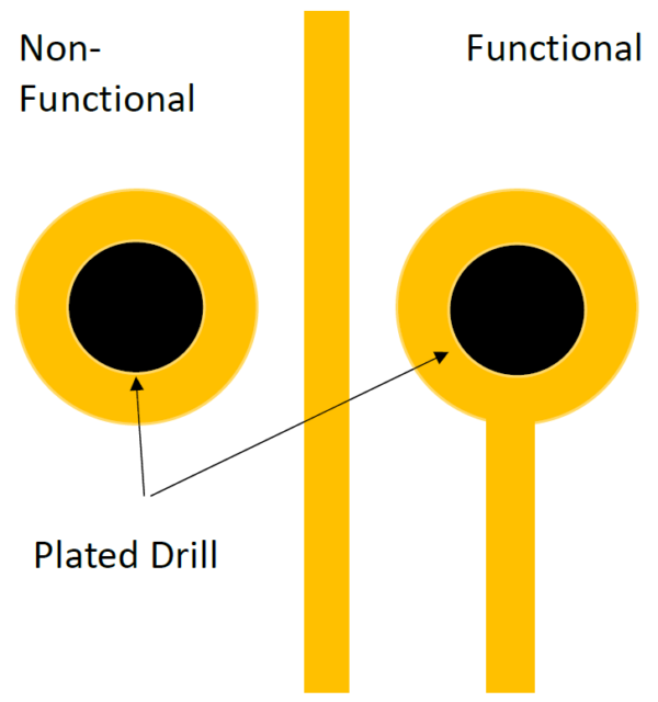
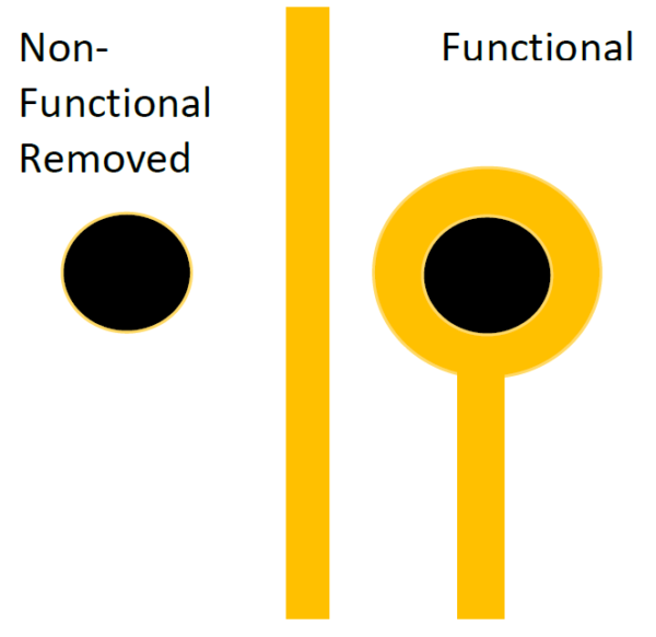
A Design with the NFP removed.
IPC-2221 Design Guideline for Printed Boards Section 10.1.3 States “Internal lands should not be removed to “make enough room” to route between holes. To help maintain internal minimum spacing, circuit routing should always be performed with all of the lands in place on all layers for each hole. After all circuits have been routed, non-functional lands may be removed.
Here is an example when the guidance is not followed in order to incorporate a second conductor between vias.
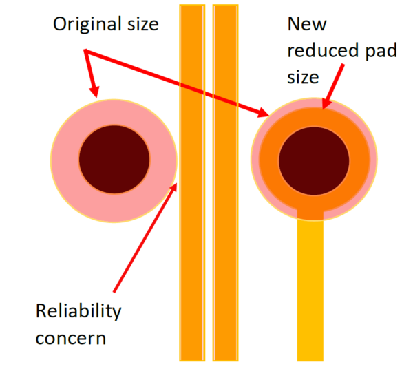
The image appears to be fine and everything would be reasonable if all the layers aligned and the drill position and quality was perfect. There are a few minor changes, the conductor width is smaller and the annular ring of the pad has been reduced, and tangency of the drill to the edge of the pad might be allowed.
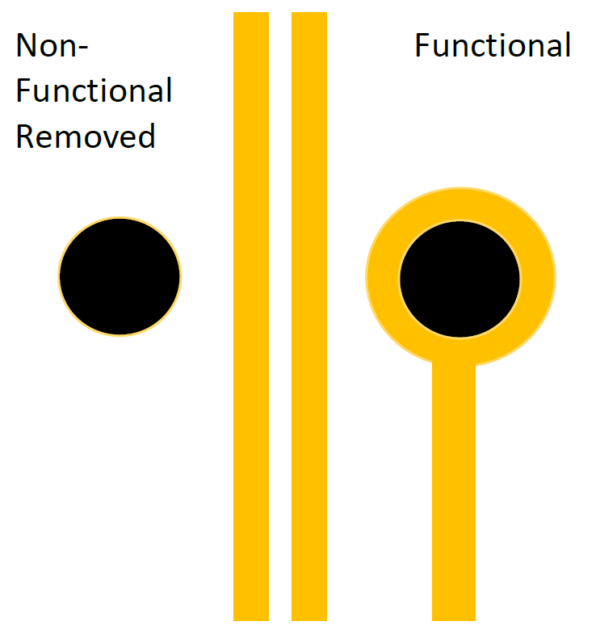
Here is the same image with the original pad and conductor sizes in light red, if everything is perfect there appears to be sufficient space between the NFP location to the nearest conductor highlighted as “Reliability concern”.
Now to illustrate what is allowed in the manufacturing of a PCB and the danger to reliability of the finished PCB.
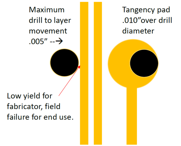
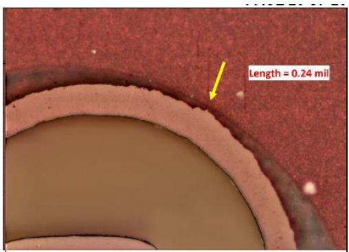
For IPC-6012 class 3 acceptance, an inner layer requires a minimum on .001” annular ring. Typical annular ring budget for a class 3 design is .006”. Class 2 allows for 90 degree of breakout of the drill. Typical recommendation for tangency for the first lamination cycle requires a .005” annular ring.
The next image takes the last image and shifts .005” which illustrates worst case of a layer movement, multiple lamination movement and drill wander.
If a short occurs in fabrication, the manufacture may find the defect at electrical test and reject the part.
This leads us to a more dangerous situation when the PCB doesn’t actual fail electrical test, and the part is shipped, gets assembled and goes out into the “field.”
A part that passes electrical test, can fail in the field because of conductive anodic filament CAF. This is the migration of copper between vias and it is necessary to plan for the potential of .002” growth in your design. It also necessary for the planning of “dielectric removal” and wicking. This is created by drilling, desmear and etchback operations which opens pathways in the dielectric for copper to deposit, and where CAF can potential grow in the hole wall. Here is an example with etch back with allowable smear removal and wicking.
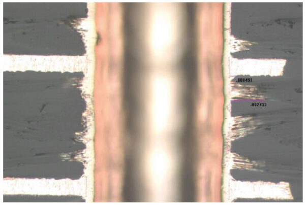
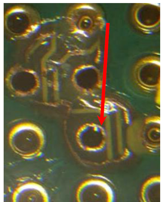
The next example is a case when the NFP pads were removed, the design had drill to copper at .007”, and the part passed electrical test. The part shipped, was assembled, tested and shipped to the field. The part later, failed in the field. Note the variation of the drill wander.
To be successful, rout the conductors with via pads in place.
After completing the routing, remove the pads. This will maintain the safe drill to copper spacing.
Summary:
For safe reliable designs it is best to plan for a plated hole drill diameter to copper distance at .010” or greater. Please note this is not the finished hole size but the actual mechanical drill diameter. It is possible to reduce the distance, but the yield and reliability diminish as the distance gets reduced. Leave the NFP during routing. Remove the NFP pads once routing is complete.
Just for the record there is a segment of my customer base that has drill to copper down to .00525” and these parts have been built for the last 15 years. These parts are evaluation parts and are not considered high reliability.
Well that’s it in a nutshell. Your questions and suggestions are welcome.
Stay healthy and safe everyone!
The Free Electron Model
There is an excellent chance that you don’t understand how charges move in conductors or how energy moves in your circuit. Preconceptions you’ve held since high school and college might be affecting how you layout your printed circuit boards.
Don’t worry; you stand in good company with most electronic engineers – the preconceptions that lead to bad layout practices permeate the industry.
When you imagine how charges move in a conductor, the chances are that you’ve got one man to thank for it. Over 120 years ago, Paul Drude presented a model of charge movement in a conductor that is in widespread use today. That model has perpetuated into textbooks that have taught untold numbers of physics students through the decades.

Drude’s idea is also called the free-electron model (later the Drude-Lorentz and Drude-Sommerfield model.). Virtually every high school and college physics textbook teaches conduction based on this primitive model.
In Drude’s model of conduction, charges move through a conductor in the presence of an electric field, and the electrons scatter as they move from atom to atom, much like the balls in a pinball or Plinko machine. The scattering gives rise to resistance and explains Joule heating, and those are the first equations presented and taught when the textbook transitions to the subject of current electricity.
Unfortunately, the model leads engineers to focus solely on the charge movement inside a conductor and not on the conductor’s surface or space around a conductor.
A cursory search of current physics textbooks on the shelves of the local used textbook store only produced a single undergraduate textbook that teaches electronic transport differently: “Matter and Interaction” by Chabay and Sherwood.
Drude Got it Wrong!
Drude created his model in 1900[1], just 3 years after J.J. Thomson discovered the electron[2]. For reference, Thompson proposed his “Plum Pudding” model of an atom in 1904 before Ernest Rutherford discovered that atoms had a nucleus in 1911[3]. James Chadwick didn’t discover Neutrons until 1932[4]. So while the model conforms to accepted physics models and can explain basic ideas such as incandescence, Ohm’s law, and Joule heating, the Drude model is incapable of explaining transmission line physics. Drude’s model is the one that you likely learned in school that influences your day-to-day thoughts of what happens in a conductor but there are ways to view conductors a bit differently.
Footnotes:
[1] https://en.wikipedia.org/wiki/Drude_model
[2] https://aps.org/publications/apsnews/200010/history.cfm
[3] https://aps.org/publications/apsnews/200605/history.cfm
[4] https://www.aps.org/publications/apsnews/200705/physicshistory.cfm