 Your connection to advanced PCB manufacturing
As customers and OEMs demand higher currents and increased operating temperatures, the need for heavy copper in PCB stack-ups has grown significantly. However, this presents challenges on the manufacturing side, where thicker copper layers can lead to lamination cracks or voids. Only a select group of suppliers has the specialized expertise to address these issues effectively, making it a niche area within the industry.
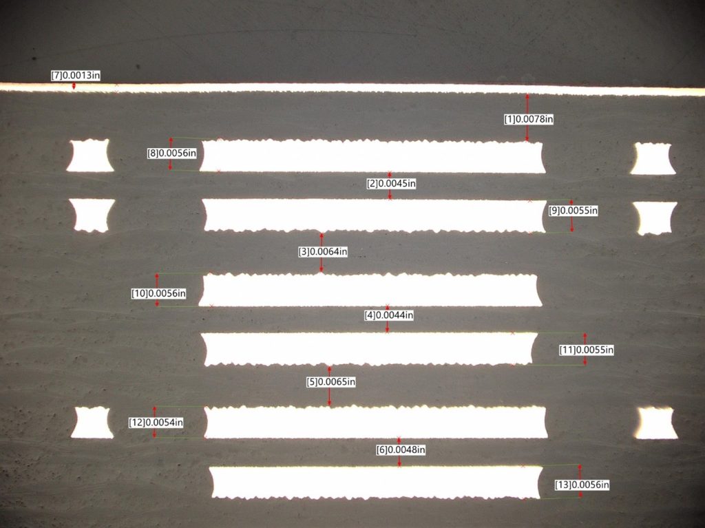
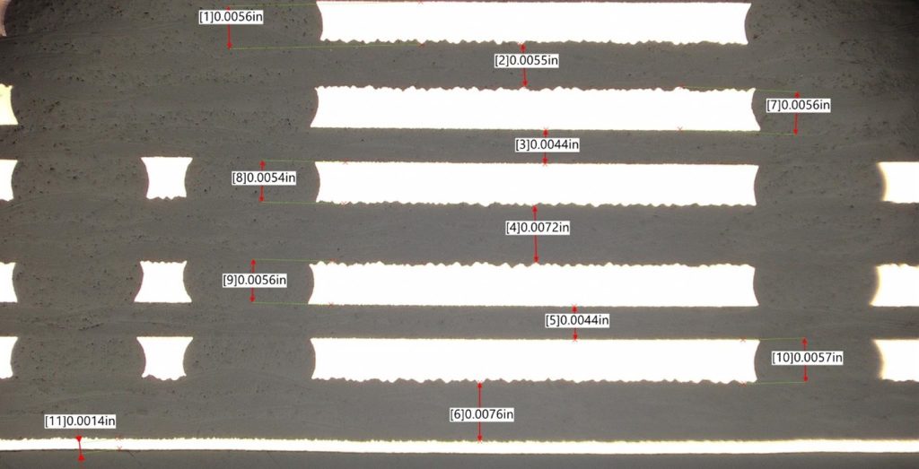
Over the years, Summit has established itself as a leader in the heavy copper lamination process, consistently delivering exceptional results. Our cutting-edge approach to heavy copper lamination enables us to expertly handle even the most demanding requirements, such as laminating 4 oz copper, while ensuring precision and quality in every aspect, including drilling. This capability allows us to meet the rigorous standards of industries that require robust and reliable PCB solutions, solidifying Summit as a trusted partner for your most challenging projects.
At Summit, we continually invest in the latest technologies and processes to ensure we stay at the forefront of PCB manufacturing. Our experienced team works closely with customers to develop tailored solutions that meet their specific performance requirements, no matter how complex. With a focus on quality control and on-time delivery, Summit has built a reputation for reliability, making us the go-to partner for OEMs and customers looking for long-term solutions to meet evolving industry demands.
IPC-6012 (Qualification and Performance Specification for Rigid Printed Boards) and IPC-6018 (Qualification and Performance Specification for High Frequency (Microwave) Printed Boards), along with the Space Addendum, all address the manufacturing standards and requirements for printed circuit boards (PCBs). Summit meets all manufacturing standards and requirements for 4 oz Copper IPC.
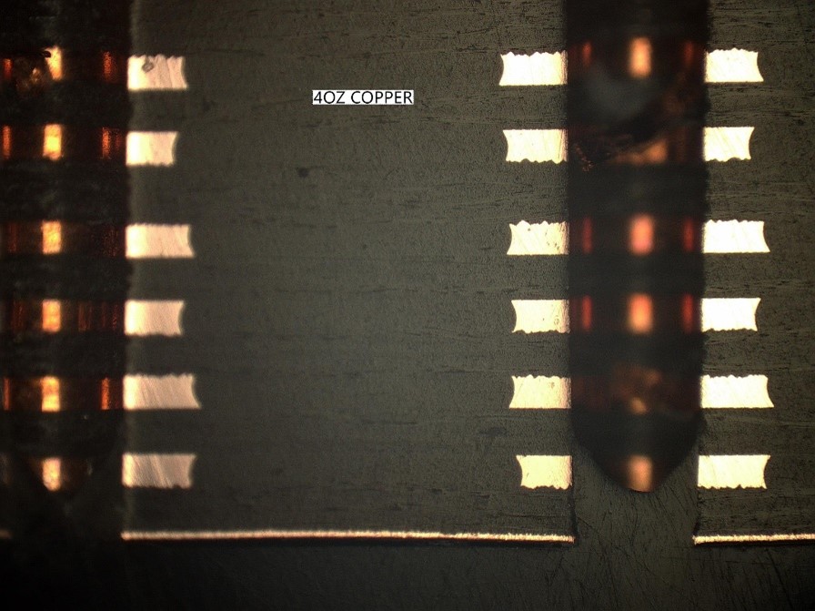
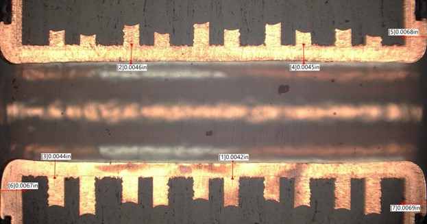
Picture below are from a 12 Layer all 4oz Copper job.
Coupon Plating
IPC has released new plating requirements to allow for finer line widths.
Table 3-10 now requires only 5µm [197 µin] minimum wrap plating for buried vias > 2 Layers, through holes, and blind vias. Prior to this revision, the minimum wrap plating requirement was 12 µm [472 µin].
This new allowance is helpful for PCB manufacturers as it provides better capability to support continually advancing fine line widths and spacing requirements found in many designs today. By allowing a thinner minimum plating requirement, PCB manufacturers may target less plating on the surface of the plated layer than the previous revision allowed. This in turn allows for better control of thin spacing requirements as there is less total copper to etch down to form copper features and spacing.
Table 3-10 Surface and Hole Copper Plating Minimum
Requirements for Buried Vias > Layers, Through-Holes, and Blind Vias
| Absolute Minimum | 25 µm (984 µin) |
| Wrap | 5 µm (197 µin) |
Note 1. Does not apply to microvias (see 1.4.4 of IPC-6012F)
Note 2. Wrap copper plating for PTHs and vias shall be in accordance with 3.6.2.11.1 of IPC-6012F. Alternatives to wrap plating shall be AABUS.
Note 3. See 3.6.2.11 of IPC-6012F.