 Your connection to advanced PCB manufacturing
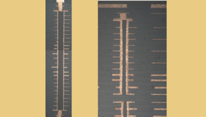
Automotive electronics have become increasingly sophisticated, requiring high-reliability PCBs that can withstand extreme temperatures, vibrations, and environmental conditions. Automotive PCB manufacturing focuses on producing durable, high-performance circuit boards essential for modern vehicles and transportation infrastructures.
Key Considerations in Automotive PCB Manufacturing
Automotive PCBs must function in extreme heat, cold, and humidity. To achieve this, manufacturers use high-Tg (glass transition temperature) materials for improved heat resistance. Enhanced thermal dissipation, while conformal coatings protect against moisture, dust, and chemicals, ensuring longevity in harsh environments.
Vehicles are subject to constant motion and impact, which makes vibration resistance crucial. Reinforced solder joints help prevent cracking under stress, while flexible PCBs are commonly used in areas requiring bending or movement. High-reliability interconnects ensure secure component attachment, maintaining consistent performance over time.
Safety and reliability standards are paramount in automotive PCB manufacturing. Compliance with ISO 26262 ensures functional safety in road vehicles, while IATF 16949 establishes a quality management system for automotive production. Components also undergo rigorous testing under AEC-Q100/AEC-Q200 standards to guarantee reliability in demanding automotive applications.
Different vehicle systems require specialized PCBs designed for specific functionalities. Engine Control Units (ECUs) rely on high-temperature, multi-layer boards for processing engine operations. Advanced Driver Assistance Systems (ADAS) demand high-frequency, low-loss PCBs for precise signal transmission. Electric Vehicle (EV) power management systems use heavy copper PCBs to handle efficient power distribution, while lighting and infotainment systems benefit from flexible and rigid-flex PCBs for compact designs.
To ensure automotive PCBs meet performance requirements, manufacturers implement advanced testing and quality control measures. Automated Optical Inspection (AOI) detects potential defects early in the process and X-ray testing analyzes hidden solder joints. Thermal cycling tests simulate real-world vehicle conditions, and high-voltage and electrical continuity tests verify the safety and performance of power systems.
Final Thoughts
Automotive PCB manufacturing demands high-quality materials, precision engineering, and strict compliance with safety regulations. As vehicles integrate more electronic features, advanced PCB technologies will continue to drive innovation in the automotive industry.
The increasing demand for miniaturized, high-density interconnect (HDI) printed circuit boards (PCBs) has made microvias indispensable for achieving compact, high-performance designs. However, designing PCBs with microvias placed over epoxy-filled and cap-plated mechanical vias presents significant reliability challenges. This article delves into the underlying failure mechanisms, offers an in-depth explanation of critical issues, and outlines strategies to improve the reliability of these structures.
Introduction
Microvias are crucial for interlayer connectivity in HDI PCBs, enabling compact layouts and advanced functionalities in aerospace, automotive, telecommunications, and other high-reliability industries. However, microvias drilled into the cap plating of epoxy-filled mechanical vias are particularly vulnerable to mechanical, thermal, and adhesion-related failures. Addressing these vulnerabilities requires an understanding of their root causes and the implementation of robust design and manufacturing strategies.
Failure Mechanisms
1. Mechanical Stress at the Cap Plating
The cap plating, a thin copper layer sealing the epoxy-filled via, is prone to structural weaknesses, especially when subjected to drilling or operational stresses.
- Thin Plating and Structural Weakness: The cap plating is typically thinner than the copper walls of standard vias, limiting its ability to withstand mechanical stress, particularly from laser drilling.
- Localized Stress from Microvia Drilling: Drilling microvias into the cap plating introduces localized mechanical and thermal stresses. Even precise laser drilling can leave micro-cracks or uneven edges that act as stress concentrators.
- Epoxy’s Insufficient Mechanical Support: Unlike solid copper, epoxy lacks the mechanical rigidity needed to reinforce the cap plating. Consequently, the cap plating bears most of the mechanical load, increasing its susceptibility to deformation and cracking.
2. Thermal Expansion Mismatch
Thermal cycling during soldering, testing, and operation imposes considerable stress on the cap plating and epoxy due to differences in their material properties.
- Differing Coefficients of Thermal Expansion (CTEs): Copper and epoxy expand at different rates under heat. Epoxy’s higher CTE creates tensile stresses in the cap plating during thermal excursions.
- Fatigue Cracking: Repeated thermal cycling weakens the cap plating, causing micro-cracks that propagate into the microvia or epoxy core.
- Localized Hotspots: Microvias over cap-plated vias hinder heat dissipation, creating hotspots that exacerbate thermal stress and accelerate material fat.
3. Adhesion Issues Between Epoxy and Copper
The interface between the epoxy fill and the cap plating is a common failure point due to weak bonding, which stems from the nature of the electroless copper plating process.
- Electroless Copper Over Cured Epoxy: After the epoxy is cured and planarized, the surface becomes smooth and lacks the micro-roughness or adhesion promoters found in standard copper foil. Electroless copper deposited on this smooth surface has inherently lower peel strength compared to copper foils.
- Absence of Adhesion Promoters: Copper foil typically includes adhesion promoters (such as oxide or oxide-reduction treatments) to enhance bonding with the underlying substrate. These promoters create a mechanically interlocked interface, significantly increasing peel strength. In contrast, electroless copper relies solely on chemical adhesion, which is less robust.
- Delamination Under Stress: The weaker bond between electroless copper and planarized epoxy increases the likelihood of delamination when subjected to mechanical or thermal loads. This delamination creates crack initiation sites, reducing both structural integrity and electrical connectivity.
4. Microvia-Specific Vulnerabilities
Microvias drilled into cap plating over epoxy-filled vias face unique challenges that undermine their reliability:
- Inadequate Foundation: Microvias require a strong, continuous copper foundation for stability and stress distribution. The softer epoxy under the cap plating fails to provide adequate mechanical support.
- Stress Amplification at Interfaces: The transition point between the microvia wall and the cap plating experiences stress concentration, making it a hotspot for crack initiation and propagation.
- Crack Propagation into Microvias: Micro-cracks originating in the cap plating often extend into the microvia walls, threatening electrical continuity and structural stability.
5. Voiding and Plating Defects
Defects in the epoxy fill or cap plating exacerbate reliability issues.
- Voids in Epoxy Filling: Gas entrapment or inconsistent curing creates voids that weaken the mechanical and thermal performance of the via.
- Inconsistent Cap Plating: Uneven or thin copper deposition over epoxy-filled vias introduces weak points prone to cracking under stress.

Consequences of Failures
The interplay of these failure mechanisms leads to several detrimental effects:
- Electrical Discontinuity: Cracks sever conductive pathways, causing signal loss or open circuits.
- Thermal Dissipation Issues: Reduced thermal conductivity weakens heat dissipation, creating localized overheating.
- Accelerated Fatigue: Stress concentration and material mismatches amplify fatigue, reducing the PCB’s operational life.
Mitigation Strategies
1. Safe Design Practices
- Staggered Vias: Avoid placing microvias directly over epoxy-filled vias to distribute stresses more evenly.
- Teardrop Pads: Use teardrop-shaped pads at the microvia entry point to reduce stress concentration.
2. Enhanced Materials and Structures
- Copper-Filled Vias: Replace epoxy-filled vias with copper-filled alternatives to provide a robust, conductive foundation.
CTE-Matched Epoxy: Use epoxy materials with a lower CTE to minimize thermal expansion mismatches. - Thicker Cap Plating: Increase cap plating thickness to improve mechanical and thermal resistance.
3. Process Optimization
- Void-Free Filling: Employ advanced techniques to ensure consistent epoxy filling and curing, eliminating voids.
- Consistent Plating Quality: Maintain rigorous quality control to ensure uniform cap plating.
4. Advanced Testing and Inspection
- Thermal and Mechanical Testing: Validate reliability under simulated operational conditions, such as thermal cycling and vibration testing.
- Inspection Techniques: Use X-ray imaging and cross-sectional analysis to detect voids, delamination, or other defects.
Conclusion
Placing microvias over epoxy-filled and cap-plated mechanical vias introduces a range of challenges that compromise PCB reliability. Understanding the root causes of these failures—mechanical stresses, thermal mismatches, and weak adhesion—enables engineers to design more robust HDI PCBs. By adopting advanced materials, optimized via configurations, and stringent manufacturing controls, it is possible to enhance the durability and performance of these critical interconnect structures.
References
- IPC-6012: “Qualification and Performance Specification for Rigid Printed Boards.”
- IPC-2226: “Design Standard for High Density Interconnect (HDI) Printed Circuit Boards.”
- Park, J., & Yoo, C. (2019). “Failure Modes in Microvia Structures Under Thermal Cycling.” IEEE Transactions on Components, Packaging, and Manufacturing Technology.
- Phan, T., & Wright, T. (2020). “Improving Microvia Reliability Through Material and Process Optimization.” PCB Design & Fabrication.
- Bhattacharya, S. (2017). “Advanced Manufacturing Techniques for HDI PCBs.” Journal of Electronics Manufacturing Technology.