A circuit operating at high frequencies exhibits opposition or impedance to flow of electric current from the combination of resistance, inductance, and capacitance present in it, when an alternating voltage is impressed across the circuit. This impedance is made up of a complex sum of the circuit’s DC resistance and its reactance. While the DC resistance is independent of the frequency of the alternating voltage applied, the reactance depends on whether the circuit element is inductive or capacitive. For an increase in frequency of the applied voltage, the circuit’s inductive reactance increases while its capacitive reactance decreases—the opposite happens when the frequency decreases.
While resistance associated with a circuit does not cause a change in the phase angle between the applied alternating voltage and the resultant current, reactance in a circuit causes the current to lag or lead the voltage, depending on whether the circuit is inductive or capacitive.
For mathematical calculations, just as circuit resistance is represented by R, electrical impedance is represented by Z, capacitive reactance by XC and inductive reactance by XL. Both inductive and capacitive reactance are expressed in ohms, similar to the units assigned to represent resistance, and therefore, impedance as well.
Why Impedance Matters in a Printed Circuit Board
For a copper trace on a PCB, the return path may be through another trace or the ground plane. While the resistance the current faces remains a constant when it courses through the trace and its return path, the impedance the current faces depends on the nature of the trace and its return path. For instance, whether the return trace does or does not follow the primary trace closely, or the return plane is close to the primary trace or far from it, changes the impedance faced by the current.
In short, unless the designer has carefully designed the trace, its return path, and their environment properly, the impedance is likely to vary in value from point-to-point along the trace. At high frequencies of the applied voltage, PCB traces seldom behave as simple connections, and the varying impedance degrades the signal as it travels around the PCB.
Just as the presence of resistance in a circuit serves to reduce or attenuate the amplitude of the current flowing through the circuit, the impedance of a PCB trace also attenuates the amplitude of the current flowing through it. However, as this attenuation is frequency dependent, it affects the circuit performance in complex ways. For instance, perfect square waves at high frequencies, when traveling through PCB traces may no longer be able to retain their vertical edges, or the corners of their waveform may become rounded.
A square wave is effectively a combination of several sine waves at various frequencies, with each being an integral multiple of the fundamental. As this combination travels along the trace, the varying impedance along the trace attenuates the higher frequencies to a larger extent than they do to the lower frequencies. Therefore, the shape of the waveform reaching the other end of the trace no longer retains the original starting sharpness, but is distorted in a manner described above.
This distorted waveform causes unpredictable problems in the functioning of the circuit receiving it, and is hence, is unacceptable. The remedy is to control the impedance along the PCB path such that the distortion at the end is negligible and the receiving circuit is able to compensate for the same, thus offering repeatable high-frequency performance.
Controlling the characteristic impedance of a transmission line formed by PCB conductors is known as controlled impedance. This becomes all the more important when high-frequency or high-speed signals propagate through PCB transmission lines. Controlling the impedance is necessary for signal integrity—propagation of signals without distortion.
Controlling Impedance
Factors that influence impedance include:
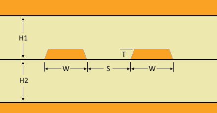
- Width and thickness of the copper trace on top and bottom of the layer
- Thickness of the prepreg or core material on either side of the copper trace
- Dielectric constant of the prepreg or core material
- Distance from other copper features
Therefore, a PCB manufacturer may have to change certain specifications such as the trace width, its thickness, and the thickness of the prepreg or core material to make sure of achieving the final impedance within the specified tolerance.
The PCB materials used by the manufacturer also define the impedance of traces. Manufacturers call the impedance of materials and the expected impedance based on them as controlled dielectric. Most manufacturers offer methods of calculating impedance based on the dielectric space necessary between the copper layers in the fab, and allow laying out the traces with the proper width and spacing. This leads to two methods of impedance control:
Controlled Dielectric: The designer specifies the PCB stack-up, dielectric material and thickness, along with tolerances. The fabricator focuses primarily on building the board with the specified thicknesses from layer-to-layer within the specified tolerance and does not attempt controlling the impedance.
Impedance Control: The designer specifies the impedance, and the fabricator achieves it by controlling the dielectric thickness, trace width and spacing. The manufacturer uses TDR coupons to test that they have achieved the desired impedance. Before committing to an entire order, the manufacturer processes the first article to evaluate any discrepancies. Depending on the results from the first article, the manufacturer adjusts process parameters to meet the designer’s specifications within the specified tolerances.
The Path of Least Impedance and High-Speed Signals
Although the path of least resistance may be a shorter one on the PCB, high-speed signals prefer to follow the path of least impedance instead. At low frequencies, the return current mostly follows the ground plane directly from the load to the source. This straight line between load and source represents the path of least resistance, and this is the path of least impedance for low frequencies as well.
With increase in signal frequency or speed, mutual inductance between the trace on the signal layer and the copper plane below it creates a low-impedance path that allows return currents to follow the trace on the signal layer.
Designing Return Paths in PCBs
PCB designers usually follow best practices that allow proper routing of signals and their return paths along the path of least impedance. Some of these best practices are:
- Return path very close and parallel to or beneath the trace carrying the high-speed signal
- Differential signals coming from package pins should immediately come close together and remain close together for their entire route
- Place ground return vias close to differential pair vias
- Tie copper pours around interconnects to ground plane below.
- Surround clock and other fast rise/fall signal traces with ground pours and use a complete, uninterrupted ground plane below the signal trace to minimize noise from EMI
- Designs requiring FCC testing may have to route high-speed signals between two ground planes, surrounded by stitched vias.
Calculating Controlled Impedance
It is also possible to calculate controlled impedance from physical parameters mentioned earlier. However, the equations are based on complex mathematics, and field solving methods such as boundary element analysis are necessary to solve the equations.
Testing PCBs for Controlled Impedance
Critical PCBs with controlled impedance undergo 100% testing. However, the actual traces making up the controlled impedance may not always be accessible for testing. In addition, the involved traces may be too short for making accurate measurements, and may also contain vias and branches that would also make it difficult to measure the impedance accurately. Adding extra vias or pads to aid testing can affect performance, and take up extra space on the board.
Therefore, manufacturers test controlled impedance not on the actual PCB, but on a few test coupons, which they integrate into the panel. The coupon follows the same layer and trace construction as in the main PCB. As the traces on the coupon have identical impedance to those on the main PCB, testing the coupon assures the manufacturer that the impedance on the board will be correct.
Measuring Controlled Impedance
The time domain reflectometer or TDR is the most common instrument for measuring controlled impedance. During measurement the TDR uses a cable and probe to apply a fast voltage step to the traces on the coupon. The cable is of a special type also with tightly controlled impedance. Any change in impedance value—a discontinuity—comes across as reflections in the pulse waveform output that the TDR displays. Appropriate software in the TDR translates the measurement data to indicate the scale and location of the discontinuity. The software in the TDR also plots a graph of the impedance along the length of the test trace on the coupon. This graph is the trace characteristic impedance, and allows making several complex measurements.
Equipment for Measuring Controlled Impedance
Several OEMs make various types of equipment for measuring controlled impedance. Among them, Tektronix and Agilent are two well-known names. For instance, modular TDRs from Tektronix allow the user to mix and match different modules for achieving the best combination required for their application. The Signal Integrity Analysis series of TDRs from Agilent allow users to apply multiple ports for the measurement. Each instrument has its own advantages and disadvantages pertaining to the application requirements.
Conclusion
With the increasing operating speed and frequency of signals in modern equipment, combined with their shrinking dimensions, achieving repeatable and consistent functioning is dependent on signal integrity and careful design of PCBs. For this, one of the critical factors is controlled impedance. Best practices in PCB design and improvements in manufacturing techniques, aided by modern instruments help in taking away most of the mystery in achieving the desired controlled impedance.
More articles

Understanding Controlled Impedance in High-Frequency PCB Design
Controlled impedance is crucial in printed circuit board (PCB) designs that operate at high frequencies ...

Sustainability in PCB Design: Insights from Summit Interconnect at IPC APEX EXPO 2025
At IPC APEX EXPO 2025, Gerry Partida, VP of Technology at Summit Interconnect, sat down ...

The Key to First-pass Success in PCB Design
In the dynamic world of PCB manufacturing, achieving first-pass success hinges on more than just ...