When designing PCBs, engineers usually assign a model number, a version number, and the version release date. Not only does this help identify a particular PCB for a specific product, the numbering system also helps with traceability as required by ISO and IPC standards. PCB manufacturers print the details on the PCB surface using a method known as silkscreen printing.
Along with the PCB details, the silkscreen can also include:
- company logos,
- manufacturing marks,
- identification number for components,
- PCB and PCBA part numbers,
- component orientation symbols,
- test points,
- warning symbols,
- RoHS compliance,
- and other marks considered important for assembly.
The Manual Silkscreen Process
The most common method of printing the information on the PCB surface is by depositing white non-conducting ink through a stencil. The manufacturer applies the silkscreen printing over the solder mask when the boards are still in their panelized form, just before routing or v-scoring.
The first step in this process is to spray a polyester screen stretched across an aluminum or wooden frame with solvent resistant emulsion. Next a laser printer creates the initial film and a UV printer imprints the image onto the emulsion. After washing with a developer and baking in the oven, the screen with image is ready for printing.
The operator has to position the screen on the panel, taking care to register them precisely for proper alignment. The operator then uses a squeegee to draw the epoxy ink across the silkscreen and panel combination. The ink seeps in through the silkscreen image onto the panel and may require oven-curing to dry.
The quality of the manual silkscreen printing process depends to a large extent on the viscosity of the ink, humidity and temperature in the room, age of the ink and hardener, and the line resolution to be printed.
LPI or DLP Process
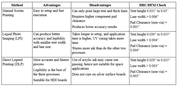
For greater accuracy, manufacturers use the LPI (Liquid Photo Imaging) or DLP (Direct Legend Printing) process. Although DLP is the most accurate, it can also be the most expensive. A comparison of the three processes is given below:
The Importance of Quality Silkscreen
Although silkscreen printing is a part of the board fabrication process, its primary use is for accurate PCB assembly. Silkscreen markings are used to help place and mount components, and for later testing and troubleshooting. Designers mainly use four types of placement markings:
- Reference Indicators — these identify the component type and number from the BOM
- Component Outline/Landing Pattern — this indicates where the component is to be actually placed
- Start Pin Indicator — this indicates the orientation of a multi-pin component to the pads of the footprint.
- Polarity Indicator — this indicates the orientation of a polarized component.
For help during testing and troubleshooting, designers can include additional markings such as:
- Test Point Indicators — these indicate test points which can be useful in primary testing of the board
- Warning Symbols — these indicate points or areas that need special care while testing as they may contain high voltages or other dangerous parameters.
- Part Numbers — these provide information on special parts.
Designing Silkscreens
Although silkscreen design is a part of the PCB design process using the CAD software, some attention to detail is necessary to create a good readable print on the board. These may be summarized as follows:
- Ensure the silkscreen is effective and useful, by making the text clearly legible and with readable fonts.
- Gerber calls the top and bottom silkscreens as Top overlay and Bottom overlay.
- All text must have the same orientation, either horizontal or vertical, as this makes it easier to read them.
- Do not allow text to overlap other texts—this improves readability.
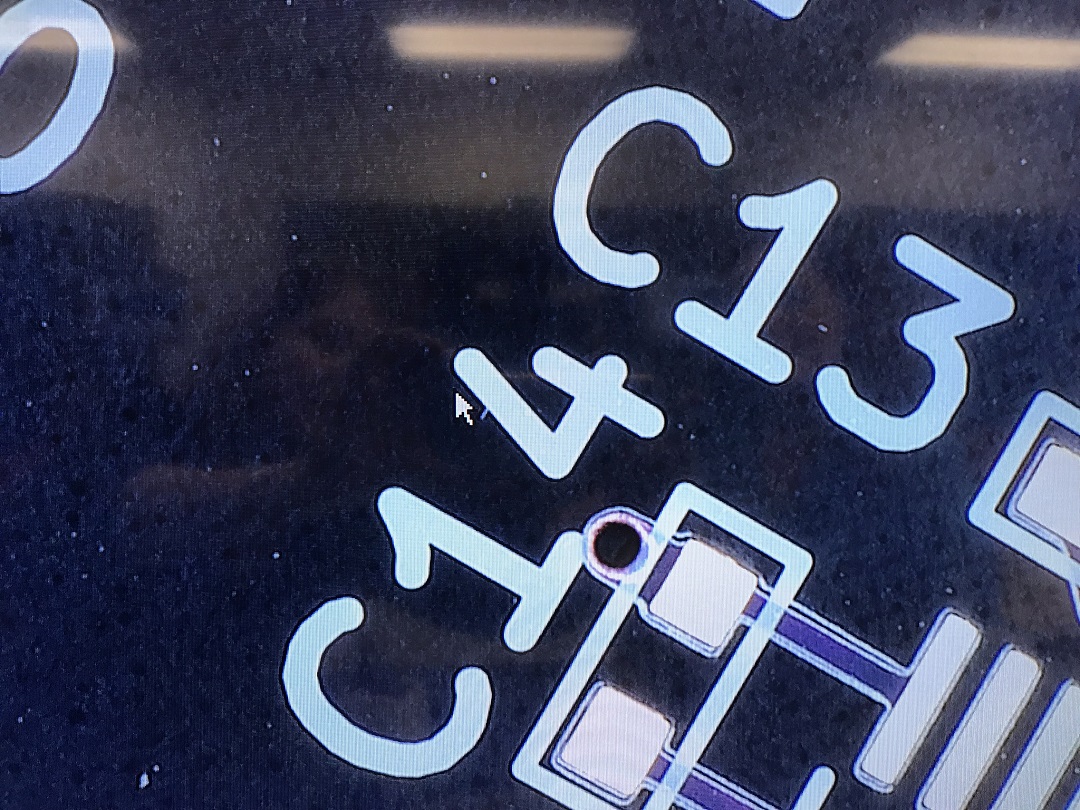
- Do not allow text to overlap onto solderable pads and vias. Ink over solderable pads can affect their solderability. Text over an untented via remains partly printed due to lack of a surface over the via, making it difficult to decipher.
- Place component reference designators, pin numbers, polarity indicators, test point indicators, and similar markings such that they are not covered by the components after assembly. As these markings help in testing and troubleshooting, they must always be visible after the board is fully assembled.
- Select an ink color to provide maximum contrast. Some fabricators, like Royal Circuit Solutions, do not charge for different color solder mask or silkscreen ink.
- Do not place text on high speed signal tracks. Placing silkscreen text on high speed signal tracks may alter the dielectric value and affect board performance.
- Avoid placing text between neighboring heavy copper pads in heavy copper PCBs.
Conclusion
With more PCBs moving towards HDI (High Density Interconnect) and Flex, with blind and buried vias on them, and component miniaturization, the quality and readability of silkscreen printing is more important than ever.
More articles

Orbital High Ground Why Space Superiority Is Slipping Away
“The next war might be won—or lost—22,000 miles above Earth.” That’s not science fiction. It’s the ...

RF & Microwave PCB Design: Navigating High-Frequency Complexity with Precision
RF and microwave PCBs aren’t just signal carriers—they’re performance enablers. In the GHz realm, every ...
How Embedded Heat Sinks Are Advancing PCB Fabrication
Managing localized thermal loads is increasingly critical as power densities rise. One solution to this ...