When an engineer orders a printed circuit board from a fabricator, the fabricator will generate a list of steps that assembly line workers must follow to create that board. This list of steps is called a traveler and it follows the project from machine to machine and from assembly line worker to assembly line worker inside the factory. Some factories use paper travelers while other factories use digital travelers.
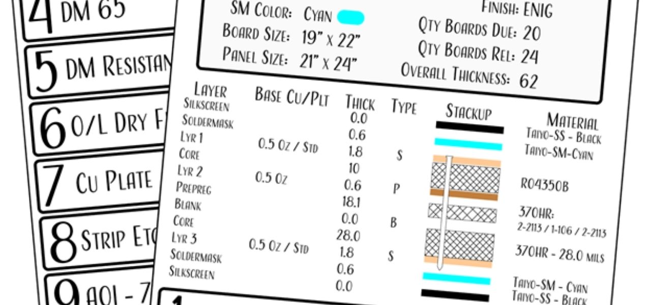
A traveler is a detailed checklist that describes each step required to make a printed circuit board.
Each step takes personnel and machine time and adds risk to the process. To keep the cost of your PCB Down to the lowest possible levels, you should do whatever you can to minimize the number of steps.
Here are a few examples:
- Avoid blind and buried vias where possible.Blind and buried vias are made the same way as through-hole vias, however, they are made in extra processing steps from through-hole vias. Blind and buried vias require additional lamination cycles and additional electroplating cycles to create.
- Limit your lamination cycles.Copper cores and copper foil are joined together in a hot-oil press. There, enormous pressures and controlled temperatures cure the epoxy pre-impregnated (“prepreg”) fiberglass and permanently bond the copper foil layers together. Each time your panel goes into the press, the dielectric layers are damaged slightly, and there is always the risk that the foil layers can fall out of alignment. Always use the least number of layers possible in your design.
- Avoid laser-drilled micro vias where possible.Almost all boards have mechanical drills, but only HDI boards require microvias. New drill machines have machine-vision capabilities that allow for smaller annular-rings on normal-thickness PCBs, which means unless you are dealing with <0.65mm pitch components, you might be able to use mechanical drills and avoid lasers. Note that mechanical drills are through-hole, they don’t have the single-layer depth that lasers offer.
Talk to your fabrication partner today to find out how they can help you with your next design.
Would you like to learn more about the fabrication process? Contact info@summittinterconnect.com to speak with Summit’s technology team!
More articles

Orbital High Ground Why Space Superiority Is Slipping Away
“The next war might be won—or lost—22,000 miles above Earth.” That’s not science fiction. It’s the ...

RF & Microwave PCB Design: Navigating High-Frequency Complexity with Precision
RF and microwave PCBs aren’t just signal carriers—they’re performance enablers. In the GHz realm, every ...
How Embedded Heat Sinks Are Advancing PCB Fabrication
Managing localized thermal loads is increasingly critical as power densities rise. One solution to this ...