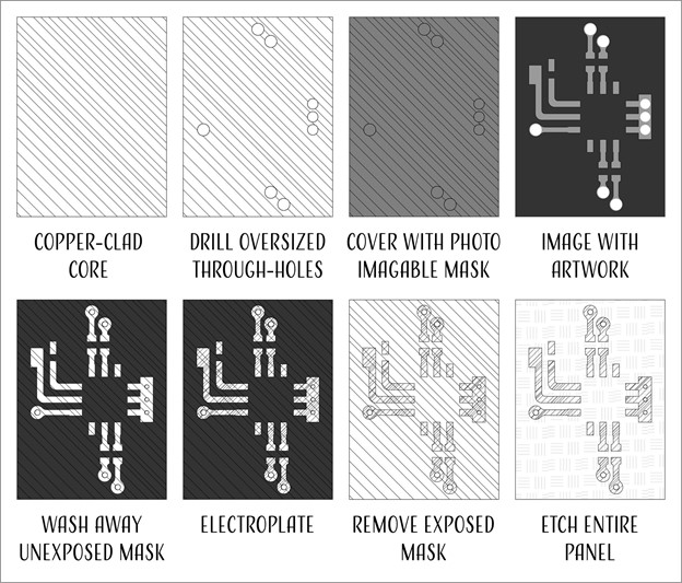
Good engineers become great engineers when they have a comprehensive understanding of how printed circuit boards are made. This quick tip covers electroplating, via formation, and etching.
- Fabricators will start with a copper-clad core or stack.
- They then drill holes in the panel that are larger than the engineer specifies — these holes will become smaller after electroplating.
- The next step is to cover the entire panel with a photo-imagable mask. This material hardens when exposed to light.
- The artwork is either projected on the panel or imaged with a line-scan laser. The light selectively hardens the material in certain areas.
- The mask material that was not exposed to light is then washed away.
- The entire panel is connected to the cathode of a pulsed-DC power supply. Copper ions leave a sacrificial ingot and deposit on the panel in the exposed areas.
- All of the mask is washed away, leaving a panel with exposed copper that is raised in certain areas that will become the traces, pads, and copper pours.
- The entire panel is placed in an etching solution that removes copper from the entire board. The parts that have thickened in the electroplating process take longer to etch, so if the board is removed at the right time, all that will be left behind are traces atop a dielectric substrate.
If you have any further questions, contact our engineering experts for more information.
More articles

Fabrication
06/23/25
Orbital High Ground Why Space Superiority Is Slipping Away
“The next war might be won—or lost—22,000 miles above Earth.” That’s not science fiction. It’s the ...

Fabrication
06/17/25
RF & Microwave PCB Design: Navigating High-Frequency Complexity with Precision
RF and microwave PCBs aren’t just signal carriers—they’re performance enablers. In the GHz realm, every ...
Fabrication
06/04/25
How Embedded Heat Sinks Are Advancing PCB Fabrication
Managing localized thermal loads is increasingly critical as power densities rise. One solution to this ...