A new thought for better PCB performance, assured compliance, reduced design time, reduced PCB fabrication time, higher yields, and reduced field failures.
As most of you know there is no 1.1mm BGA or CGA package. This post is to share my thoughts on what tradeoffs we live with now, because we are forced into a 1mm pitch, and how a slight increase in the pitch size could satisfy the needs for today’s high I/O pin count designs. This post is from my observations of building Class 3 and space 1mm pitch products for my customers, and the challenges, setbacks, redesigns, returned product, and field failures we all endure.
Ideally we would all like to have the following allowances in a design for performance, layout, compliance and yield.
- The ability to double tract conductors between via lands.
- Conductors that are not less than .004″
- Spacing between conductors not less than .004″
- Drill to copper distance of .010″
- Drill diameters of .010″ and aspect ratios less than 12:1.
- Annular ring that meet class 3 (design should have a land .014″ over the drill
size) - Meet copper plating in the hole .001″ minimum (IPC-6012 class 3)
- If via in pad, epoxy fill that meets IPC-6012
- A design that can pass OM Reflow 2.6.8 and Thermal Shock testing 2.6.27B testing approaching 100%.
Currently the 1mm pitch does not allow this, and we enter into a world of compromise and higher non-compliance results. Let’s look at what the tradeoffs are in respect to IPC-6012 class 3. Please keep in mind for these complex builds with multiple lamination cycles, and that the loss of 1 panel can be $1000-$10000 or more.
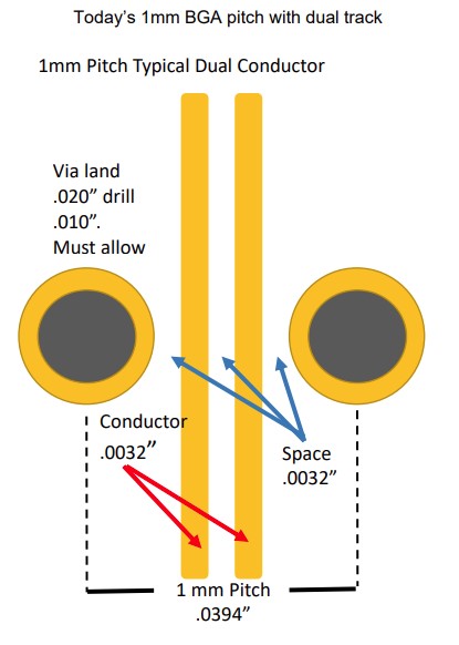
- Class 3 annular ring requirement is relaxed to Tangency or class 2. This will only gain .001″ additional space. Higher risk of breakout, non-conformance and rejection on an entire production panel.
- Drill sizes are typically reduced to .0079″ gaining another .001″ of space. Aspect ratio can be 12:1 or higher for the same thickness. The customer may need to relax copper thickness requirement, and change from long established minimum copper requirements. A failed cross section rejection will result in the rejection of the entire production panel.
- Dual conductors between via lands will have conductors that are .003″-.0034″ in the BGA package. The concerns regarding conductor resistance becomes a concern. Fabricator yields for inner layer processing drops.
- Space for dual conductors limits differential pair and dielectric options. There is little room to change values or dielectric thickness. Reduces space also reduces inner layer fabrication yields.
- Drill to copper internal signal layers. The best scenario is drill to copper distance of .009″. I highly recommend .010″ or greater for reliability and field life. Here is the reason for a distance of .009″. Layer and drill registration will take up to .005″ of distance in a typical build. Dielectric removal (etch back, wicking, drill quality) typically will take .002″ IPC-6012 allows .00315 for class 3″, so with normal conditions we have used up .007″ of our .009″ spacing budget. Lastly IPC-2221 guidelines requires .002″ minimum (worst case condition) distance between 0-50volts. We have now arrived at the value of .009″
- Drill to copper plane layer this has the same distance rule, except the designer would like additional copper on the plane return for impedance. The impedance conductor edge is typically exactly over the plane clearance edge since they have the same exact design distance to the drill.
- Via pad and epoxy filling a .0079″ drill bit might not meet IPC-6012 60% fill requirement. Entire production panel can be rejected for a non-conformance condition.
- OM testing failures can increase with the smaller diameter vias.
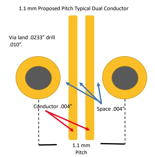
Here is conceptually how a 1.1mm pitch device provides the Win-Win for everyone inthe supply chain.
- The Pitch is now .0433″
- The via land size is .0233″ with a .010″ drill.
- Design annular ring .0067″. Assured meeting tangency, best in class fabricators will meet class 3.
- Assuming PCB thickness is .100″ aspect ratio 10:1, no plating issues
- Can be epoxy filled compliant to IPC-6012 60% fill requirement.
- Dual conductors with .004″ conductors and space.
- Higher manufacturing yields
- Allows for impedance line, space and dielectric flexibility
- Drill to copper for signal layers .0107″ assuming .0067″ annular ring and .004″
land to conductor space. - Drill to copper can be set to .010″ and allow for “wider” copper return for impedance line. This adds .0007″ which is better than the zero oversize that currently exists for dual conductors on a 1mm pitch.
I can only imagine the impact this size package could have in our industry. I have seen many programs suffer and re-spin the design just to get to the point that fabricators are yielding parts in the 70% range. I have seen whole programs cancelled. It seems to me that we have been forced to use package sizes dictated by semiconductor providers, who frankly have never designed or fabricated a PCB. In preparation for this post I read several semiconductor’s design guidelines for 1mm grid pitches and I thought I was reading fiction this Saturday morning. One even recommended a drill to
conductor space of .007″ for designers. Naturally I hit the comment button and used words like egregious.
So let’s consider a different package size other than a whole number (1) we did it for .8mm, .65mm and other pitch sizes. Yes, I understand the package is bigger. For example, a 40×40 1600 I/O 1mm grows from 1.575″ to 1.732″, but I have also seen that there is generally enough room around these large packages and in almost all cases could allow for the larger package.
More articles

Orbital High Ground Why Space Superiority Is Slipping Away
“The next war might be won—or lost—22,000 miles above Earth.” That’s not science fiction. It’s the ...

Bipartisan PCBs Act to Revitalize the Microelectronics Ecosystem
Washington, May 27, 2025 – The bipartisan Protecting Circuit Boards and Substrates Act of 2025 introduced ...

Empowering the Next Generation of Tech Innovators in Electronics
The electronics industry is at the heart of technological progress, driving innovative advancements that shape ...