Every Electronic Design Automation (EDA) tool is a bit different. Some have more features than others, some have different features, some offer simulation, some don’t. But they all have a few features in common: they allow designers to capture a schematic and layout a PCB.
In a schematic diagram, components are represented as abstract symbols.
On a printed circuit board, components are attached to copper pads arranged in carefully designed land patterns.
To create a design, you need a part library that has all of your components’ land patterns associated with the components’ schematic representation.
Basic EDA Structure
There are four basic parts of every EDA tool. The pattern editor, component editor, schematic layout, and PCB layout program. The names of the modules might vary from program to program, and they might be used differently, but they all exist in one form or another.
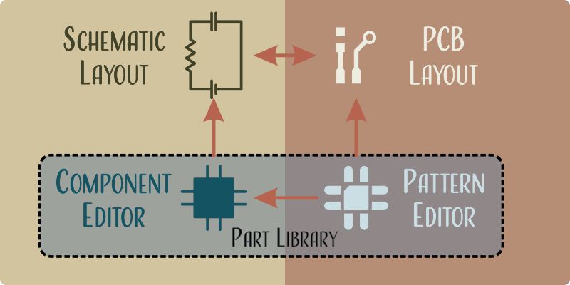
- Component editors alter the appearance of schematic symbols.
- Pattern editors alter the appearance of land patterns.
- Libraries hold collections of linked components and patterns for reuse from design to design.
- Schematic Layout arranges the connections between components.
- PCB Layout arranges the patterns and the traces that connect them.
Libraries hold groups of footprints and components. When a component is selected for use in a schematic, it’s associated land pattern is prepared for use in the PCB layout portion of the software.
Pattern Editor
Engineers use the term footprint to describe the outline of the bottom of a discrete component and its pads/pins.
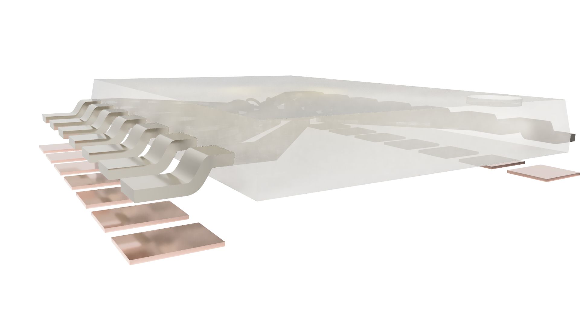
To make things even more exciting/confusing, the land patterns associated with those pads are often incorrectly called footprints by engineers, even though the metalized lands have to be larger than the metalized pads/pins they mate with.
Discrete components have metalized pads or pins on their base and sides.
Printed circuit boards have metalized lands on their outer layers.
These two metalized parts have a similar pattern but are two different sizes. Solder connects the lands to the pads/pins.
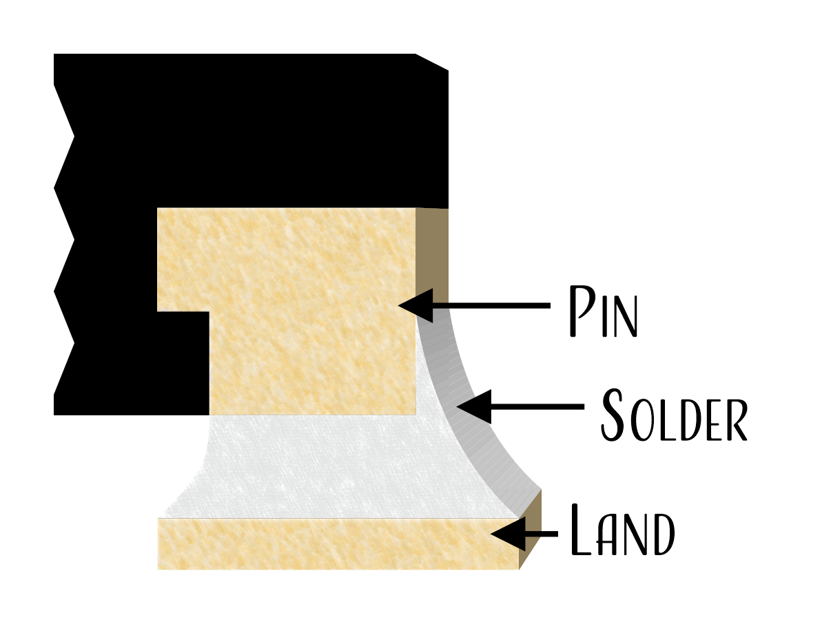
For a proper solder joint to form, the solder has to form a filet, and the only way that can happen is if the land is bigger than the pad/pin.
A discrete component’s metalized pad pattern and a printed circuit board’s land pattern are identical in layout and centerline spacing, but the metalized lands are always bigger than the metalized pads.
The size and shape of footprints and lands has been largely standardized into IPC-7351, a document that describes the pin pattern, layout, and naming convention for all standard parts.
Component Editor
The abstract symbols that represent PCB components are created and edited in a component editor. Components are shapes that abstractly define the function of a physical part, with pins that represent metalized pads/pins on physical components. There are two standards in broad use and as long as the symbols don’t jump from one standard to another within a schematic document, it’s usually pretty easy to keep track of what is going on.

Schematic Capture
Schematic Capture is the part of the program that takes the components from the library and lays them out on a document. Parts are connected with virtual wires that allow designers to see the electrical connections between pins. A set of pins that are electrically connected is called a net.

When you pull a component from the library, you should do two things.
Make sure the part is available. It’s very common for EDA part libraries to be out of date and include parts that are now obsolete and unobtainable.
Double-check the land pattern that is associated with the part number is correct. You never know who made the library entry, and it’s possible that they read the datasheet incorrectly or they copied the footprint in a 1:1 manner.
You should go through a careful schematic review process before you move on to layout. Even the simplest schematic is complicated. Errors caught at the schematic stage can save hours of rework at the layout stage.
PCB Layout
While you have been layout out your schematic, your EDA has been quietly been keeping track of your land patterns, and the connections between the pins. If it’s been set up properly, there’s a good chance that it knows which pins require special routing rules as well.
More articles

Understanding Controlled Impedance in High-Frequency PCB Design
Controlled impedance is crucial in printed circuit board (PCB) designs that operate at high frequencies ...

Sustainability in PCB Design: Insights from Summit Interconnect at IPC APEX EXPO 2025
At IPC APEX EXPO 2025, Gerry Partida, VP of Technology at Summit Interconnect, sat down ...

The Key to First-pass Success in PCB Design
In the dynamic world of PCB manufacturing, achieving first-pass success hinges on more than just ...