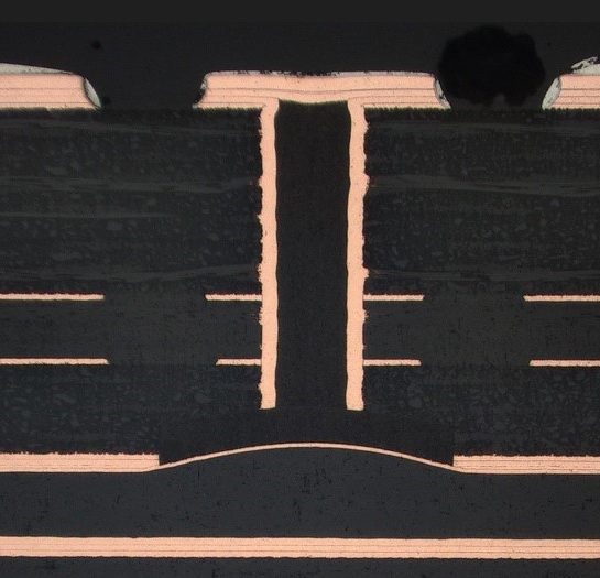
IPC has released new plating requirements to allow for finer line widths.
Table 3-10 now requires only 5µm [197 µin] minimum wrap plating for buried vias > 2 Layers, through holes, and blind vias. Prior to this revision, the minimum wrap plating requirement was 12 µm [472 µin].
This new allowance is helpful for PCB manufacturers as it provides better capability to support continually advancing fine line widths and spacing requirements found in many designs today. By allowing a thinner minimum plating requirement, PCB manufacturers may target less plating on the surface of the plated layer than the previous revision allowed. This in turn allows for better control of thin spacing requirements as there is less total copper to etch down to form copper features and spacing.
Table 3-10 Surface and Hole Copper Plating Minimum
Requirements for Buried Vias > Layers, Through-Holes, and Blind Vias
| Absolute Minimum | 25 µm (984 µin) |
| Wrap | 5 µm (197 µin) |
Note 1. Does not apply to microvias (see 1.4.4 of IPC-6012F)
Note 2. Wrap copper plating for PTHs and vias shall be in accordance with 3.6.2.11.1 of IPC-6012F. Alternatives to wrap plating shall be AABUS.
Note 3. See 3.6.2.11 of IPC-6012F.
More articles

Orbital High Ground Why Space Superiority Is Slipping Away
“The next war might be won—or lost—22,000 miles above Earth.” That’s not science fiction. It’s the ...

Bipartisan PCBs Act to Revitalize the Microelectronics Ecosystem
Washington, May 27, 2025 – The bipartisan Protecting Circuit Boards and Substrates Act of 2025 introduced ...

Empowering the Next Generation of Tech Innovators in Electronics
The electronics industry is at the heart of technological progress, driving innovative advancements that shape ...