Communication Protocols
Serial data moves through a circuit from source to destination as a series of changing voltages. The sender(s) initiates the change on the signal line and the receiver detects that the potential has changed.
There are a variety of protocols that are in common use in the industry: ATA, SCSI, CAN, I²C, SPI, UART, RS232, RS485, USB, Ethernet, Microwire, 1-wire, etc… But commercial sensors predominantly use I²C and SPI.
Synchronous
Synchronous communication requires a minimum of two signal lines: one line transfers data, the other transfers the clock signal.
Asynchronous
Asynchronous communication requires a minimum of one signal line. However, the clock frequency must be agreed to by both the sender and receiver before communication can be successful.
I²C
The Real-Time Clock, BNO055, and BME280 all communicate with the ATMega328 via I²C.
The Inter-Integrated Circuit (I2C or I²C) protocol uses two data lines: clock and data. The Serial Clock Line (SCL) transmits the timing information while the Serial DAta line (SDA) transmits the bits of data. Either the master or the slave can trigger the data line, but only the master controls the clock. This allows for half-duplex communication between master and slave.
Advantages
One of the advantages of the I²C protocol is that it is a multi-master, multi-slave protocol. Several microcontrollers can be on a bus and read the same sensor data, provided they aren’t both controlling the clock signal at the same time. Usually, I²C is used by a single microcontroller to communicate with several slaves, such as EEPROM, sensors, displays, etc.
Disadvantages
Address Collisions
Many of the devices on the I²C bus have 7-bit addresses. With only <128 possible addresses (2^7=128, but not all addresses are used), it’s entirely possible to select two devices with identical addresses. Fortunately, most manufacturers provide a workaround by adding an address (ADDR) or multipurpose (MP) pin to their design that allows designers to change the address by changing the logic level of a pin.
Capacitance
A second disadvantage is that high bus capacitance negatively impacts the maximum data rate. The I²C bus is meant for relatively slow, short-distance communication on a single board. While it can sometimes tolerate transmission via discrete wire connections to other boards, it is not designed for that purpose, especially at high speeds.
I²C Engineering Considerations
I²C master devices will pull the logic-signal directly to ground potential and allow the pull-up resistors to bring the logic levels to Vcc potential. The logic-high to logic-low transition is fast and looks quite a bit like a square-waveform on an oscilloscope. But the logic-low to logic-high transition is mediated by the bus capacitance and the selection of pull-up resistors.
In the case of the I²C example, the RC-constant of the logic-high transition is the limiting factor in bus-speed. The resistance is provided largely by two pull-up resistors as well as a minor amount of trace resistance. The capacitance is the sum of trace capacitance, pin capacitance, and any other stray capacitance along the signal path. The I2C specification limits the maximum capacitance to 400 pF for standard (100 kHz) and fast mode (400 kHz), and 500 pF for fast mode plus (1 MHz). 400 pF is not a lot of capacitance. An individual I/O pin might have a capacitance of 2-10 pF, and a 6 mil trace increases capacitance by a little less than 2 pF/inch in FR-4 material above a ground plane.
Binary Logic
Binary logic has two states: high and low. The logic high state of an integrated circuit might be any potential difference between 70% and 100% of Vcc, and the logic low state is often any potential difference between 0 and 30% of Vcc. In between 30% and 70% the logic is undefined. (These aren’t the only logic thresholds, but are a good starting point for explanation sake.)
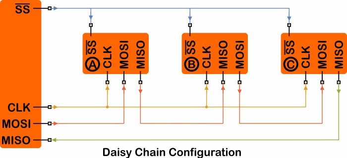
SPI
The ATMega328 communicates with the display through the SPI bus.
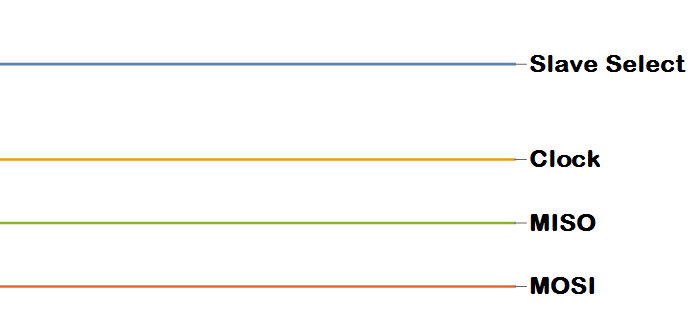
The Serial Peripheral Interface (SPI) is a bi-directional, synchronous data transfer protocol. This protocol requires at least three data lines, Master In Slave Out (MISO), Master Out Slave In (MOSI), and Clock (CLK). An optional data line called Slave Select Not is used to enable or disable data transmission on one or many integrated circuits. The overline indicates that the logic for this digital input is inverted: slave select is active, and a chip is enabled, when the logic is low. In many designs, this digital input can be tied to the ground net to permanently enable the data bus.
Data that is stored in a linear shift register is moved over bit by bit with each clock cycle. SPI is a full-duplex protocol — the sender and receiver can both transfer data at the same time.
![]()
If you were to watch the signals transition on an oscilloscope — you would see data on both the MOSI and the MISO lines.
The Universal Serial Bus specification relies on differential pair signaling to transfer data along its length at high speeds. A differential pair consists of two digital signal lines that have the same amplitude but opposite polarity.
Design Rules
For a differential pair to work as intended, the individual traces need to have consistent width and have consistent spacing to other conductors, and the two traces should remain as identical as possible — following an identical path and have identical length. The general idea is that a Low→High transition needs to propagate along the wire parallel to and at the same time as a High→Low transition. The electric fields are confined tightly between the two traces if the two signals travel the same distance over the same dielectric.
If the traces/wires are not the same lengths, or if the impedance changes in the surrounding environment, the symmetry between the two wires is lost, and one transition will lead or lag the other. When the two wires have the same polarity, the electric fields repel and can spread further from the wires.
Electromagnetic interference is the result of rapidly changing electromagnetic fields. If the field lines in the first animation switch to look like the second animation, or back again, the electromagnetic field disturbance will propagate outwards from your traces to other areas of your circuit, or into the broader environment. So the purpose of differential-pair routing is to ensure that the two wires stay as symmetric as possible over as equal a distance and as short a distance as possible.
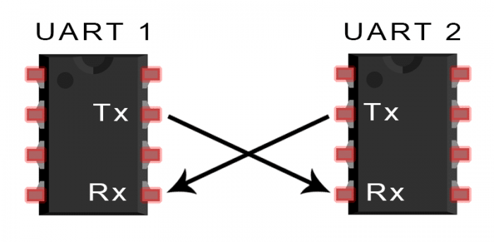
UART
The Universal Asynchronous Receive and Transmit protocol allows full-duplex communication between two nodes. The only requirement is that the two nodes agree upon a common transmission rate (BAUD rate).
Unlike the other communication protocols used in our design, UART requires a cross-over connection. Transmit→Receive and Receive→Transmit.
Since it has a relatively slow transmission rate, UART data lines can run the full length of an entire PCB panel and off-board through several meters of wiring without much an issue.
Asynchronous communication nodes are usually tolerant of a slight timing mismatch. But if the transmission rates are too different than receiving rates, the information ends up garbled. If you ever see random characters or no characters on a serial-debug screen, the usual culprit is a timing mismatch.
More articles
Understanding Controlled Impedance in High-Frequency PCB Design
Controlled impedance is crucial in printed circuit board (PCB) designs that operate at high frequencies ...

Sustainability in PCB Design: Insights from Summit Interconnect at IPC APEX EXPO 2025
At IPC APEX EXPO 2025, Gerry Partida, VP of Technology at Summit Interconnect, sat down ...

The Key to First-pass Success in PCB Design
In the dynamic world of PCB manufacturing, achieving first-pass success hinges on more than just ...