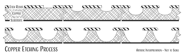
Etch Progression
Copper foil does not etch right angles to a board surface. Initially, only the exposed copper surfaces react and are washed away by the etchant, largely dissolving material perpendicular to the board surface. Then, as the etchant progresses from the etch resist layer to the substrate layer, there is increased opportunity for lateral material removal. After some time in the etching tanks, liquid etchant removes copper both perpendicular and parallel to the board surface.
At the early stages of the etching process, cross-sections of unprotected copper surfaces appear circular, and then trapezoidal with curved legs, and after extended etching, the sides may appear almost vertical.
The progression from curved to vertical requires extra time in the etch tanks and the removal of larger-than-normal amounts of copper. Fabricators do not over-etch traces to the point of verticality unless it is specifically requested by a PCB designer.
Copper Etch Compensation
After etching, the copper closest to the etch-resist layer is generally narrower than the copper nearest the substrate layer. To ensure adequate copper width after etching, fabrication houses must adjust copper artwork before fabrication in a process called etch compensation. Based on the copper weight, fabricators will expand copper features into available space by 1-8 mils, so that after etching, the width of the trace meets a specified minimum.
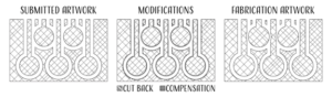
Copper Cut Back and Compensation
Closely packed copper features can interfere with this compensation process. Enough room must exist between copper features to allow the etchant to move freely into an area and copper atoms to move out. To allow adequate etch compensation on critical features, fabricators will sometimes trim the copper away from other nets in a cut-back process.
The Process
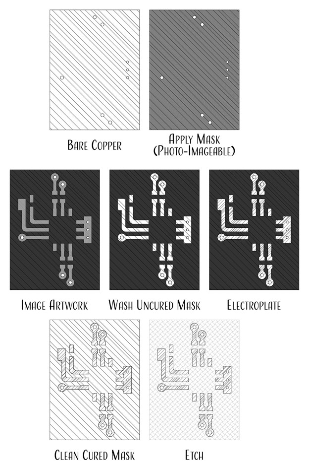
After through-holes are drilled in a panel, copper foil is covered with a photo-imageable etch resist liquid or dry-film mask and then exposed to light in a negative 1:1 pattern of the layer artwork. The light causes chemicals in the mask to polymerize and harden. The unpolymerized mask is washed away and the panel is then attached to the cathode of a pulsed DC power supply and submerged in electroplating tanks where copper accumulates on the exposed copper. The remaining solder mask is then removed from the panel.
At this point the copper foil is thicker in the parts of the board that will eventually be traces, copper pours, etc… In the last step, the entire panel is etched — copper is removed from the entire board. The thinner, un-plated areas of copper etch completely away before the thicker electroplated foil, so after etching, the traces and the copper pours are left behind.
There are a few more details to the process that were not discussed here, such as via fill, electroless catalysts, and more. To learn more, contact Summit’s technology team.
More articles
Understanding Controlled Impedance in High-Frequency PCB Design
Controlled impedance is crucial in printed circuit board (PCB) designs that operate at high frequencies ...

Sustainability in PCB Design: Insights from Summit Interconnect at IPC APEX EXPO 2025
At IPC APEX EXPO 2025, Gerry Partida, VP of Technology at Summit Interconnect, sat down ...

The Key to First-pass Success in PCB Design
In the dynamic world of PCB manufacturing, achieving first-pass success hinges on more than just ...