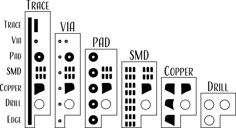
Every fabrication shop has a list of design rules that they provide to customers that detail the limitations of the manufacturing process. The specific numbers used will depend on the fabrication shop that you use as well as whether you are using their recommended process limits or their actual process limits. Remember that the closer that you get to the actual process limits, the more expensive your design will be to produce. Included in the rules are distances between traces, board edges, pads, etc…
Space Width
You set the spacing between copper features in your design program and then have the software check your PCB layout against the numbers. This is the “Space Width” part of Trace and Space width. Remember that different copper weights have different trace and space minimums, so if you have thicker inner layers of copper, you’ll want to provide separate rules for those layers.
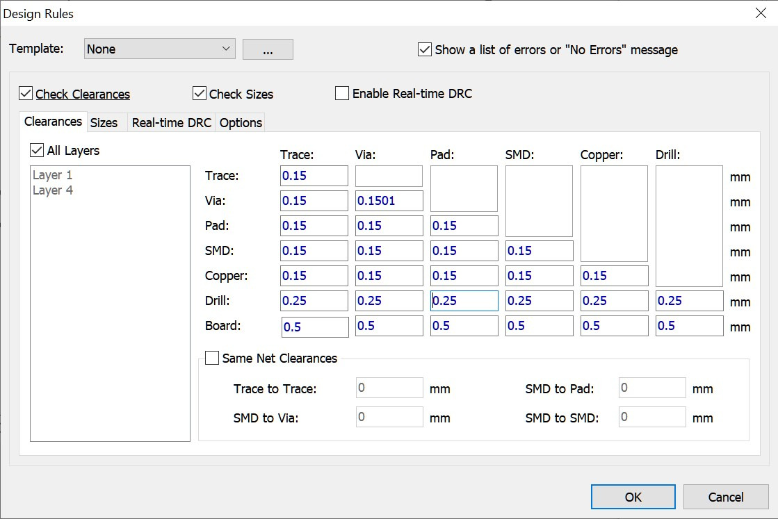
All of these values reference the minimum distance between two PCB features. Remember that PCB fabrication has some imperfections associated with it. If you take everything to the absolute manufacturing limits, then your board yield per panel will decrease.
Notes:
- Most of the values in the trace/space charts are limited by manufacturing minimums associated with copper weight. You might consider making templates based on common copper weights (0.5 oz, 1 oz, 1.5 oz, 2 oz, etc…) and then simply assign the template to each layer of your design based on your stackup.
- Metric and Imperial measurements don’t often convert well in the various EDA programs. Since layout is most often done in metric measurements, you might consider metric layout rules.
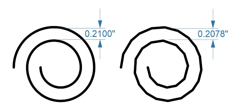
- You might consider giving yourself extra clearances. Some round shapes such as copper pour fillets, spirals, circles, etc… will be converted into straight-line segments or polygons by your EDA program. The straight-line segments that make up the line will move towards other features on the concave side of the curve — this creates DFM errors — by using numbers a few percent higher than manufacturer recommendations, you can avoid this problem.
Trace Width
Copper clearance isn’t the only concern. You also need to ensure that your minimum copper trace widths are met, there is a minimum size drill hole, minimum annular ring, etc… These are determined by the minimums provided by your design house.
More articles

Understanding Controlled Impedance in High-Frequency PCB Design
Controlled impedance is crucial in printed circuit board (PCB) designs that operate at high frequencies ...

Sustainability in PCB Design: Insights from Summit Interconnect at IPC APEX EXPO 2025
At IPC APEX EXPO 2025, Gerry Partida, VP of Technology at Summit Interconnect, sat down ...

The Key to First-pass Success in PCB Design
In the dynamic world of PCB manufacturing, achieving first-pass success hinges on more than just ...