PCB Design: Plated thru hole annular ring Class 2, Class 3 and Tangency “Class 3 light.”
This post will share, from a fabricator’s perspective, best practices to achieve first revision success in regard to IPC-6012 requirements and IPC-2221 design guidelines.
Background: This post is to help PCB designers understand how the actual drill diameter differs from the fabrication drawing specified finished hole size, and the impact on the required annular ring to fabricate a compliant printed board. Additionally, this post will share best practices for documenting vias and component-plated holes that clearly indicate finished requirements while allowing the printed fabricator the highest latitude to achieve compliance with the highest possible yield.
First the basics, “what is an annular ring”? An annular ring is defined differently between the outer layers and inner layers. For outer layers, the minimum annular ring is the minimum distance from the inside side of a finished plated hole to the shortest distance on the outer layer land.
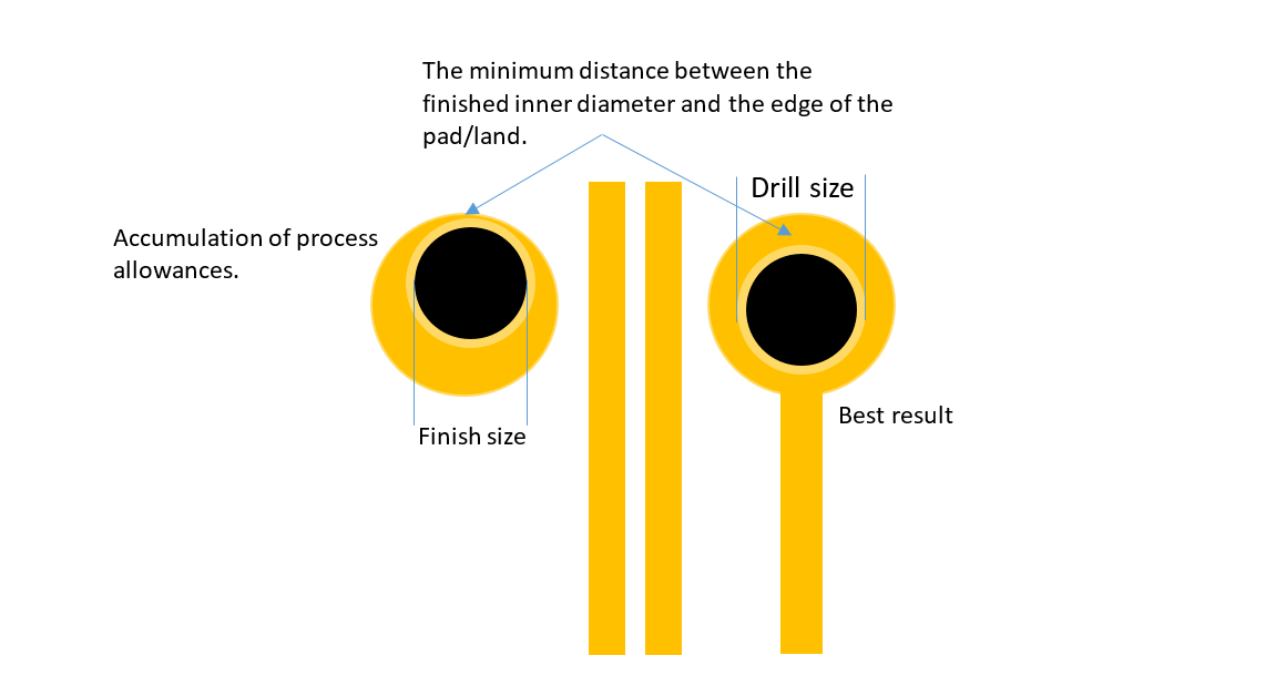
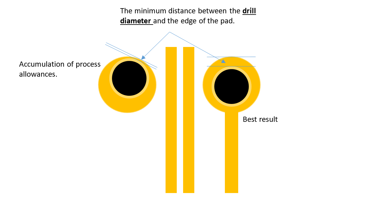
Inner layer annular ring is based on the drill diameter and the shortest distance to the edge of the drilled land. Finished hole size is not considered.
Now that we have reviewed the observable differences between outer and inner annular rings, let’s review the IPC-6012 revision E table 3-9.
Class 3 external layer minimum allowed annular ring is .001969”, measured from the inner diameter of the finished plated hole to the shortest edge of the plated land.
Class 3 internal layer minimum allowed annular ring is .000975”, and is measured from the drill diameter to the shortest distance to the edge of the land.
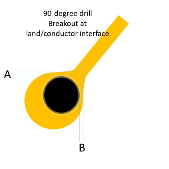
Class 2 allows for 90 degree breakout as long as there is a teardrop/filleting/keyholing at the land conductor junction. Here is an illustration to help explain what is allowed and what is required.
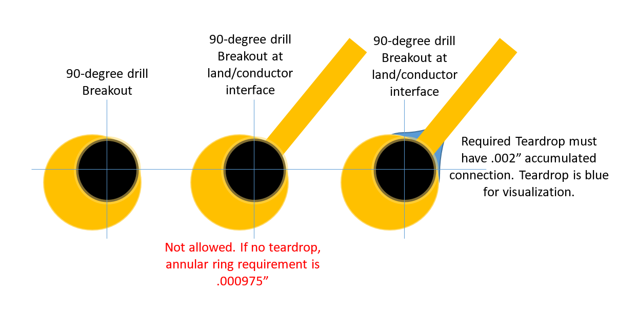
With increased densities, many class 3 designs cannot achieve a minimum .000975” minimum annular, but also cannot accept 90-degree breakouts for high reliability. A useful comprise is the allowance of tangency as long as teardrops are added to the land/conductor interface.
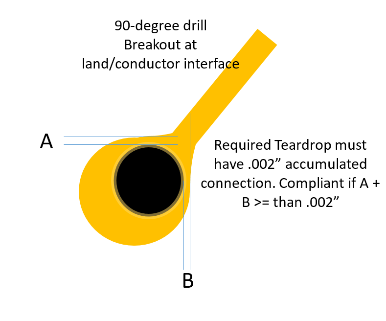
Several of my customers affectionately call Tangency “Class 3 light”. At this time the condition is not classified for mechanical plated holes in IPC-6012 or IPC-A-600. If you choose this option in your design, you will need to make a specific note for this allowance. This condition is known as an AABUS condition (As Agreed Between User Supplier).
The second part of this post is to help designers determine how much annular ring is required. This value will depend on the complexity of the design. To supplement this section, I would recommend that designers review IPC-2221 section 9.1.1, all of 9.1.2, and table 9-1.
As a designer, if you have ever had a fabricator call and inform you that the design does not have enough annular ring for compliance, this section will help you to understand why the fabricator requires adequate annular ring when it would appear that there is enough currently in the design.
To start off, registration of a drill and the lands on all the layers are not a perfect process. Here is a simple breakdown of processing tolerances and why they exist.
- Material, epoxy woven material that we purchase varies both within the lot, and from one lot purchased to the next. This variation is typically about +/-.0002” per inch. If you take this value across the working area of a production panel, you will find a variation range at .0025” on each side of a production panel.
- Front to back registration of a modern Laser Direct Imaging system is typically .001”.
- Post etch punching of an etched core accuracy is .001” at best.
- Lamination pinning and tooling adds another .001” of tolerance.
- IPC-2221 table 9-1 provides guidance to increase the annular ring .001” if the layer count is greater than 8.
- Drill machine zero position and drill run accuracy can add .001” of increased tolerance range.
- Drill bits can wander. The top layer drilled is accurate, but all drill wandering will impact the lower layers in the stackup.
- Multiple sub lamination constructions will add an additional .002” of tolerance when multiple sub-lamination structures are laminated into the final assembly.
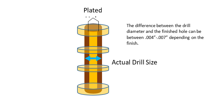
Please note the following values are based on the actual drill bit diameter NOT the finished hole size.
When we look at the accumulated process values we will divide the tolerance in half. This can be halved since we split the error across the production panels. So if we add everything together for a high layer count single lamination cycle the process allowance can be .0045” for tangency. If the job has multiple lamination cycles, the allowance for tangency would be .006” for the final drill.
If you are considering Class 3 then the annular ring value would increase an additional .001” – so for a single lamination cycle we typically ask for a .006” annular ring. For multiple lamination cycles we will allow a .006” annular on the first sub-lamination cycle but will ask for .007” annular ring on the following lamination cycles.
The last item for designers to consider is the drill size the fabricator actually drills with. To answer this question, it would be beneficial if the designer had two rules. One rule for plated vias in which the finished hole size does not matter and a second rule for component hole sizes that typically have a lead in finished plated hole. Component holes should list the finished hole size and the allowed tolerance.
Vias should be stated as vias and that the finished hole size may finish to any size less than the specified drill size. Most designs list the via size that matches the actual drill bit size the fabricator should use. Using the actual drill bit size will provide the correct annular ring and a “safe” keep back distance between a drill bit and a different net. To clearly convey that a particular drill is a via, the designer should use the following tolerance in the drill chart. This examples uses a .010” via size.
Drill X .010” +.002”/- drill diameter.
This instruction makes it clear to the fabricator that the designer implies that the design has been configured and checked with a .010” drill bit. A fabricator can look at this requirement and make a determination which drill bit will provide the best yields as long as the finished hole is .012” or less. In some cases a fabricator will drill larger if there is plenty of annular ring, or they may elect to drill smaller to ensure that the finished part will have compliant annular rings.
Component holes’ values can vary between fabricators. For component holes, a fabricator must compensate the drill size for plating and variations of the hole size after all fabrication processes have been complete. Below are the typical values, and these values should be considered during the DRC checks in CAD:
- For immersion finishes, like ENIG, ENEPIG or Silver, the drill size is .004” bigger than the finished hole size.
- For hot air solder level (HASL) finish, the drill will be .006” larger than the finished hole size. HASL cools down in an ununiformed manner and closes down the finished hole size.
- Tin Lead plate reflow may be drilled .007” larger than the finished hole size. During the reflow process this can close down the hole more than HASL.
- If a higher hole plating thickness is required it will be necessary to increase the manufacturing drill bit diameter to meet the additional plating requirement.
Summary: My intent of this post is to help designers to achieve error-free designs that go from your CAD system through our CAM systems with no DRC findings. I hope this information will be beneficial to keep your future designs free of issues that otherwise would be caught at the fabricator.
Gerry Partida
Summit Interconnect
More articles

Orbital High Ground Why Space Superiority Is Slipping Away
“The next war might be won—or lost—22,000 miles above Earth.” That’s not science fiction. It’s the ...

RF & Microwave PCB Design: Navigating High-Frequency Complexity with Precision
RF and microwave PCBs aren’t just signal carriers—they’re performance enablers. In the GHz realm, every ...
How Embedded Heat Sinks Are Advancing PCB Fabrication
Managing localized thermal loads is increasingly critical as power densities rise. One solution to this ...