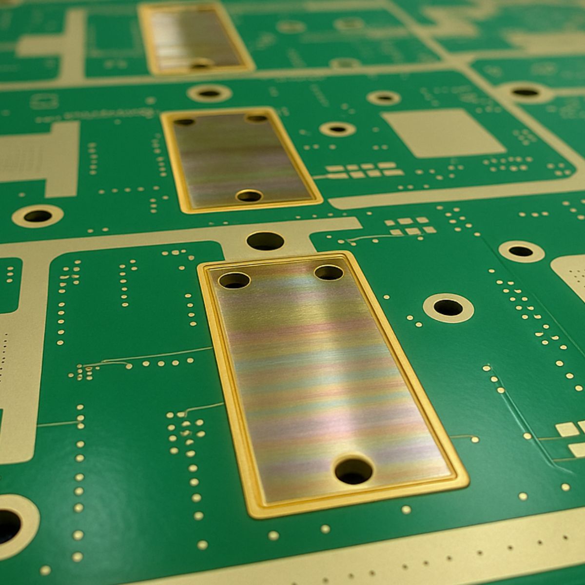
Apart from copper and solder, a Printed Circuit Board (PCB) may consist of a combination of different materials including Polyamide, Teflon, epoxy, acrylic adhesive, Kapton, aramid fibers, and glass. Each of these materials has a different relative hardness, and along with the mounting media such as acrylic or epoxy, it is obvious that micro-sectioning a PCB is not an easy task. Micro-Section Analysis or Cross-Section Analysis is one of several inspection processes to measure the quality of a circuit board.
Micro-Section Analysis is an effective tool for failure analysis as well as in-process verification. It is a threefold inspection tool for checking the internal makeup of a PCB. In general, the product specification set by the customer also contain the inspection criteria for the Micro-Section Analysis. However, the analysis may also follow standards such as the IPC 6012 and/or MIL-PRF55110/31032.
The inspector can take the section directly from the board itself, or from coupon sets produced along with the production boards. IPC 2220 series of specifications define coupon design with the intention of reflecting the design of the board. Most test coupons are usually small boards with the same number of layers and similar trace makeup as the main PCB has, both being produced simultaneously. Therefore, the use of coupons is a reliable and correct method for testing the manufacturing quality and consistency. As they reflect the process effects on the whole panel, using coupons eliminates the need to sacrifice an expensive production board only to verify the board meets necessary criteria.
Capabilities of Micro-Section Analysis
Although a destructive sample testing procedure, the PCB fabrication industry widely uses Micro-Section Analysis, as it allows them to see inside the PCB and make precise measurements to check the production processes for confirming the quality of the finished PCBs.
Typically, Micro-Section Analysis can help to check the quality of:
- The base material of the PCB
- Build checking in multi-layer boards
- Hole-wall plating thickness in a plated through hole
- Thickness of external and internal conductors
- Registration of external and internal pads
- Connection between layers
- Thickness of Surface Finish
- Thickness of Solder-mask or Coverlay
Manufacturers perform the Cross-Sectional Analysis at different stages of PCB manufacturing such as:
- After drilling, they look for internal registration and hole quality
- After plating, they look for barrel and wrap thickness
- During final quality analysis, they look for overall thickness, final registration, plating requirements, and defects.
Creating the Micro-Section
Manufacturers use through-hole coupons to determine the above. Therefore, it is essential they complete the cross-sectional preparation of the PCB in an area within 10% of the center of the plated through hole. It is common to utilize an automated coupon extraction station with a precision CNC router-cutter for extracting the test coupon.
Depending on whether it is for lot verification, vendor qualification, failure analysis, or regular conformance, precision router-cutter machines can accurately cross-section buried and blind via holes down to 1 mil or 25 microns, along with solder joints and SMT devices. After selecting the appropriate test coupon, the manufacturer cuts out a piece for the sample, immerses it within resin or soft acrylic, and allows it to harden in the shape of a hockey puck.
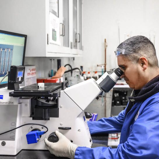
The manufacturer then grinds the hockey puck to get a flat surface, polishing the surface and etching back if necessary. The process allows easy viewing of the cut side of the board under a microscope for detailed inspection.
Analyzing the Micro-Section
Build-Checking: When checking the build-up of a multi-layer PCB, the inspector uses the Micro-Section to check the thickness of the cores, prepregs, copper foils, and the effectiveness of the process of bonding between the layers. They also look for defects in the layers caused by thermal stress, including cracks, voids, blistering, and delamination.
Wall Plating Thickness in PTH: In addition to multiple non-destructive measurements of the wall thickness of the plated copper in the hole for every production PCB, manufacturers also make regular measurements with Micro-Sections to keep a further check on process quality. For this they place a test coupon on every production panel.
In practice, the inspector takes six measurements in total, three on each side of the hole. He/she takes the measurements roughly at a quarter of the length from the top, near to half the total length, and about three-quarters down. The plating thickness is the average of the six readings.
Thickness of Conductors: As PCB manufacturers do not plate inner layers of copper, the inner layer thickness visible in the Micro-Section is that of the copper foil itself. As cleaning processes take off some copper from the foil, the remaining copper should conform to the minimum acceptable copper foil thickness after processing, as specified by IPC A 600 Class 2.
Copper on the outer layers gets a plating when the manufacturer plates the through holes. Therefore, the final thickness visible in the Micro-Section is that of the starting copper foil less the copper lost due to cleaning plus the plating. The final copper thickness should conform to the minimum acceptable thickness of finished copper after processing, as specified by IPC A 600 Class 2. From the Micro-Section it Is also possible to measure the thickness of the base copper and of the plated copper.
Hole Registration: By viewing the Micro-Section under a microscope, it is easy to check the registration of inner copper pads and anti-pads to the drilled hole, and to see if this is within the specified tolerance. Usually, manufacturers use a special test coupon with all multi-layer production panels to check the position of drilled holes in relation to the inner layers.
Connection between Layers: In practice, the wall of the plated through hole should have a robust connection to the inner layer of copper. However, process issues such as inadequate hole-wall cleaning and improper drilling can result in a poor or broken connection, which shows up in the Micro-Section analysis. An electrical test would also be able to detect such a broken internal connection within a finished board.
Surface Finish: Analysis of a suitable Micro-Section allows measurement of the thickness of Lead-free HAL or Hot Air Leveling. However, for ENIG or Electroless Nickel Immersion Gold, as the gold thickness is typically less than 0.1 µm thick, the Micro-Section will only allow measurement of Nickel thickness. Non-destructive X-Ray measurements are necessary to measure the thickness of immersion gold or immersion silver.
Solder Mask: It is also possible to use Micro-Section Analysis to measure the thickness of the Solder Mask or Coverlay over the copper conductors. For Solder Mask the minimum thickness is usually 8 µm. Coverlay thickness may vary from 12 µm to 50 µm.
Traceability with Micro-Sections
It is very important for the manufacturer to identify the panel of the lot where the coupon was fabricated, as this helps in separating the poor product from the good ones. For this, the manufacturer must use suitable markings on the coupon and the boards. The markings enable traceability for process records and further serve to identify the processing parameters for possible involvement in future failures.
Failure Analysis with Micro-Sections
Micro-Sections also serve as an effective tool in failure analysis. Evidence of internal failure may require sectioning of individual boards. Visual inspection and systematic analysis of individual Micro-Sections help to identify the problem related to the internal failures.
Specific cross-sectional views of copper thickness, pads, and solder mask usually reveal defects such as over etching, improper registration, poor solder mask thickness, and many other defects that often lead to a rejection of the PCB.
Manufacturers use the data collected from Micro-Sectional Analysis of single or numerous lots of panels for improving their processes and for validating the different processing steps they use when fabricating PCBs.
Conclusion
As PCB manufacturers shrink hole sizes, use multiple plating cycles, and increase layer counts, they realize the importance of Micro-Section Analysis for verifying the results of manufacturing processes. As a result, many now maintain a laboratory of Micro-Sections, train their staff in analysis, and provide a timely communication regarding results of Micro-Section Analysis.
More articles

Orbital High Ground Why Space Superiority Is Slipping Away
“The next war might be won—or lost—22,000 miles above Earth.” That’s not science fiction. It’s the ...

RF & Microwave PCB Design: Navigating High-Frequency Complexity with Precision
RF and microwave PCBs aren’t just signal carriers—they’re performance enablers. In the GHz realm, every ...
How Embedded Heat Sinks Are Advancing PCB Fabrication
Managing localized thermal loads is increasingly critical as power densities rise. One solution to this ...