And you should vent with me.
HDI designs and solid or near solid copper ground planes, baking and design considerations.
Over the last year we have noticed unusual delamination events with HDI designs especially with co-planar wave guides or co-planar high speed digital designs. The designs that have failed contain many HDI vias with many combinations of drill spans, with wide areas of no copper relief in the plane layers or very little. The design condition will typically have many rows of ground stitching that are plated shut microvias with epoxy filled or blind via structures. This combination of high layer copper percentage retention and the processing of microvias, blind/buried or epoxy filled vias create a condition where processing moisture becomes trapped in the dielectric between plane layers. If there is no copper relief in the layers vertically, then the only way to bake the moisture out is through the side of the PCB. This could include very long distances that may require upwards of 24-72 hours of baking to “move” the moisture out of the PCB.
So, the question is why hasn’t this happened in the past? Typical a plane layer has 85% or less retained copper across the plane layer. Without HDI or blind vias each plated hole that spanned from the top to bottom layer would have connections on some plane layers, and clearance on other plane layers. All signal plated holes would have a clearance in both plane layers. The signal layers typically would have 15% retained copper all of which were signal plated connections. Given these attributes there were always a vertical pathways for moisture to be baked out of the dielectric. All that was necessary was to bake above boiling for 6 hours and the moisture was removed or reduced to such a low volume that there was no potential to cause delamination during assembly.
A look into why HDI and highly retained copper layers can lead to delamination results during reflow.
Copper Foil
Did you ever wonder why we use copper thickness by “ounce” units? The story I am told is that copper weight in ounce units comes from the roofing industry. The prime objective for using copper as a roofing material is to prevent rain(moisture) from getting into a building. The copper foil at 93% or greater works as a very effective moisture barrier. HDI designs with plated shut microvias or with or without blind/epoxy filled vias may lack vertical pathways.
Creating Coaxial Circuitry
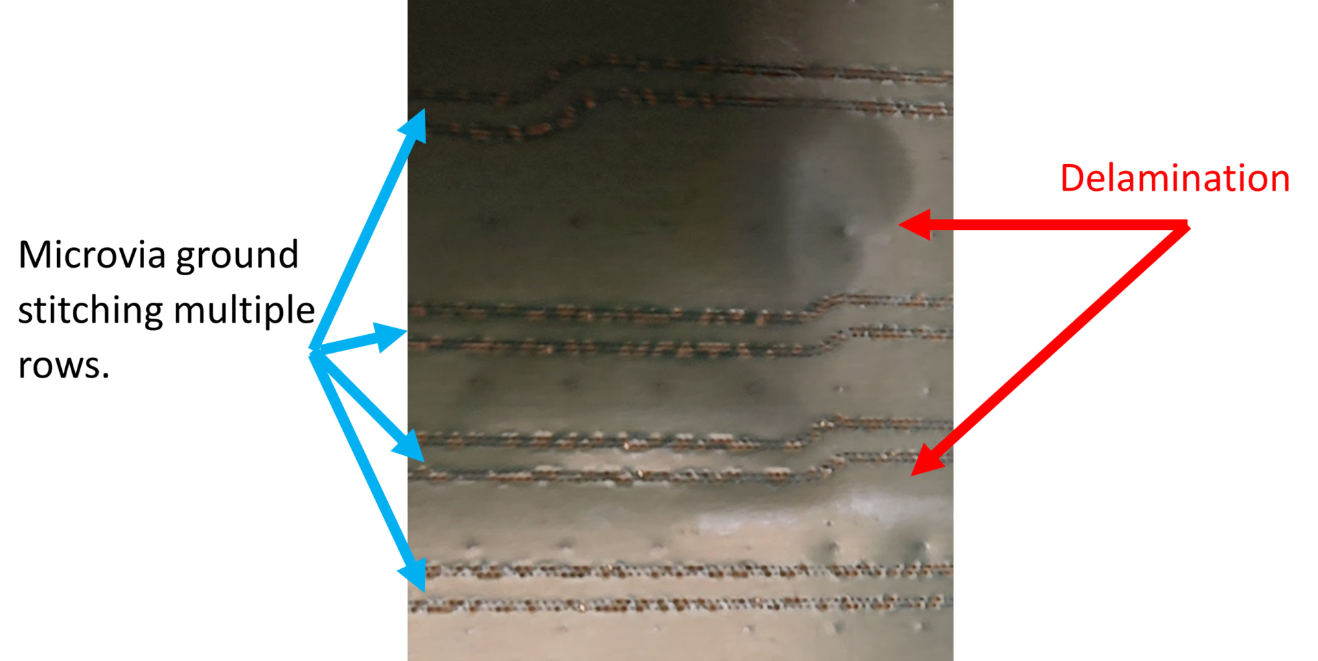
In the quest to suppress signal noise and higher coplanar performance designs, solid plane layers with no copper relief are used with ground stitched vias. The challenge occurs when many layers of microvia stitching and multiple rows of microvia are employed in a design.
Source of the Moisture
From the moment a laser drill formation has finished, the hole embarks in about 30 wet process steps before the hole wall has electroplated copper and sealing the side walls of the via. At this point the moisture that has permeated into the laminate has been stored between the plane layers (over 93% retained copper) and multiple rows of ground stitching vias. The multiple rows of ground stitched vias act as a restrictor that retards and slows the movement of moisture. To prevent the delamination the moisture needs to be removed or reduced to a safe level. It has become painfully obvious is that the moisture is trapped between plane layers above and below the dielectric and restricted from laterally moving through the multiple rows of plated ground vias.
How much moisture can get into a microvia?
Let’s do the math. If a microvia is .008” in diameter and the dielectric thickness is .005” thick. The amount of exposed area to intake moister is .000125 sq/inches. In the case the design has 50k ground stitching vias the amount of combined surface area is 6.25 sq/inches. At each wet process between laser drilling and the first electroplating process (30 steps) the 6.25 inches/sq is intaking moisture. Once the microvia has been electroplated the moisture is trapped until a very long bake cycle can be employed.
If the design has 200k microvias the amount of surface area that can intake moisture is 25 sq/inches.
How to Mitigate the Challenge
Copper pour where it is required but allow copper relief in the plane layers outside your coplanar waveguide. The relief does not need to go across the entire PCB, but a vertical pathway in the near vicinity will do the trick.
Allow for more copper relief in the planes away from the coplanar waveguide sections in the design.
Reduce the amount of ground stitching rows or the amount of vias to the bare necessity.
Extend baking cycle time to 24-72 hours as needed. This is not ideal for the surface finish condition and there is an increased concern of oxidizing the surface finish before assembly.
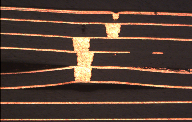
If the moisture is not removed before assembly, the chance of a delamination will exist. Other examples of delamination due to HDI multiple rows of ground stitching and plane layers with over 93% retailed copper area.
More articles

Understanding Controlled Impedance in High-Frequency PCB Design
Controlled impedance is crucial in printed circuit board (PCB) designs that operate at high frequencies ...

Sustainability in PCB Design: Insights from Summit Interconnect at IPC APEX EXPO 2025
At IPC APEX EXPO 2025, Gerry Partida, VP of Technology at Summit Interconnect, sat down ...

The Key to First-pass Success in PCB Design
In the dynamic world of PCB manufacturing, achieving first-pass success hinges on more than just ...