Welcome to my second post of hopefully many other posts that will help to demystify some common every day PCB Design rules that are well documented in an IPC document. And please if you find a rule that is badly documented, please notify IPC or better yet join a committee. By helping to improve the documents we will all benefit from designs with less holds and higher yields. Hat tip to my colleague Phil Ramon who inspired this post.
Section 10.1.4 actually is a very basic section, and the focus of this post is the first two sentences. There are two points that I would like to share in this post. Both items are important, but the second one is the most impactful to yield and reliability.
It states:
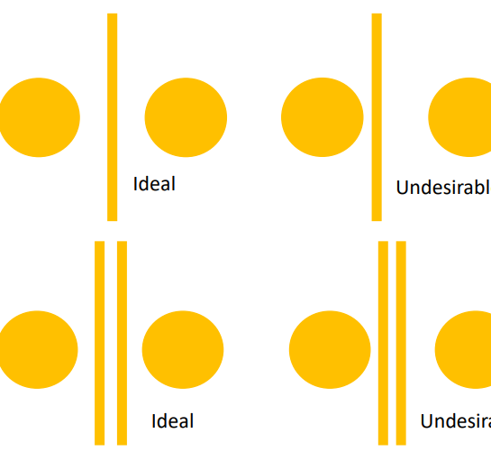
“Minimum spacing between conductors, between conductive patterns, and between conductive materials and conductors shall be defined on the master drawing. Spacing between conductors should be maximized and optimized whenever possible (see figure 10-3)”. In figure 10-3 the word “undesirable” is used.
Part 1
Minimum spacing between… conductors shall be defined on the master drawing. The bold is in the document and not my enhancement. This is an important attribute on the fabrication drawing for the fabricator to understand the complexity of the design. The minimum conductor width should also be specified. Please note this is the DESIGNED minimums and should be stated as such. It is also recommend that the fabrication drawing also state what is the minimum allowed finished conductor and space widths. Designers should also verify the spacing on the fabrication drawing matches the design data. If the drawing states a .1mm/.004” space and the design has spaces below that value, your job will go immediately on hold, and should be requoted for the increased difficulty of the design.
Example for defining design minimums and finished minimums.
Design Minimum conductor width is .127mm/.005 inches.
Design Minimum conductor clearance is:
External: .127mm/.005 inches.
Internal: .1mm/004 inches.
Finished Conductor line width of end product shall be within .05mm/.002” of digital data.
Or state the absolute minimum allowed for the finished PCB. Please note that is not the value of your
designed minimum.
A. Minimum finished conductor line width: .089mm/.0035”.
B. Minimum finished conductor spacing: .089mm/.005”.
Part 2
Spacing between conductors should be maximized and optimized whenever possible.
Here is my own illustration of figure 10-3 with my own modification to help explain “undesirable”
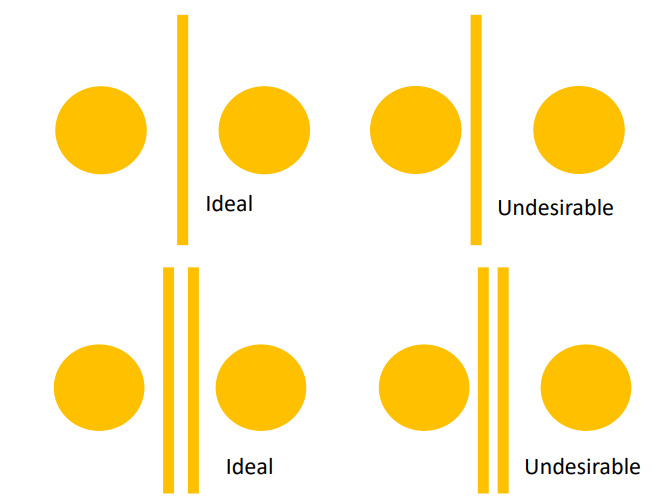
From my illustration it is self-evident that the undesirable has less space and did not maximize the available spacing. (It is interesting that IPC-2222 rev B uses the words desirable or undesirable 19 times). What I would like to share is what the impact of the undesirable usage of conductor space for PCB fabrication, and your design.
During a conversation with Rick Hartley I had this month he shared that explaining IPC rules and the impact on fabrication yields was beneficial and encouraged me to continue to do so. So the following is credited to Rick and his insight.
As a PCB fabricator we document our yields and design attributes that relate to any particular defect. For shorts, one of the attributes is the designed conductor space. We know that the yields drop when the space is smaller. Here is an example when I was visiting a customer with two part numbers with the identical components and design density. One part had a right side purpose and the other the left so they were identical mirrored parts. When we built the two parts one was delivered on time and at quantity and the other needed a remake and was delayed. The customer asked if we would opine why there was a difference. When I reviewed the yield information of both high layer count, multiple Ideal Undesirable Ideal Undesirable laminated, very densely designed HDI PCBs, I found that the higher yielding PCB had .089mm/.0035” space, and the other PCB was designed with a space of .076mm/.003”. The final yield difference was 5%, which was just enough to cause a remake and the delay. The point of this example is that every opportunity that exists to increase space should be done as stated in IPC-2222 section 10.1.4. Will it take longer to design? Why yes, but the original layout is only done once, with very little or no spacing modification for following revisions. The design is done once, but we fabricators have to process each layer and each image with greater or lesser yields. The impact of unnecessary finer spacing will increase the cost of your PCB. The minimum space is a direct cost adder for the product life of each PCB design. The other impact that is normally not considered (but should be) is the waste of material, processing time, and money for remakes simply because the available spacing was not maximized or the minimal spacing was not utilized only in the components that needed a finer space.
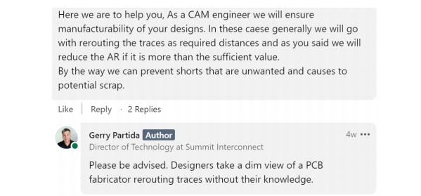
And now for the dirty little secrets that designers don’t know could happen. I will start by saying I DON’T EMPLOY THIS PRACTICE, but I know it exists. (I was a CAM Application Engineer, and visited over 100 PCB sites and trained many of them). There are fabricators that will simply reroute your conductors to increase spacing. I once saw a customer’s CAM operator making reroute edits and asked him “does the customer know you are modifying the routes,” and his answer was “the customer can’t see since the reroutes are hidden by the ground planes on layers 2 and X-1.” Don’t believe me? Here is a screen shot that a fabricator replied to a recent post of mine stating that he reroutes the conductors. Name has been removed to protect the guilty.
Also there are amazing spacing rerouting tools in the PCB fabricators CAM software. (I absolutely forbid the usage of these feature in our CAM departments). It can reroute all of the conductors and your time matched networks in seconds, and all of it outside of the designer’s controls. So if your design’s timing works from one supplier and not the other, it is possible that CAM operator moved your conductors to gain spacing.
Outside Design Services:
Outside design services can reduce the cycle time by setting spacing to the absolute minimum throughout the design and speed up the design cycle time. Translation: the design is finished faster and the invoice can be sent sooner. I’m not saying all design services act this way. There are many excellent services that apply IPC-2221 section 10.1.4 religiously, but 9 out 10 times I can tell the difference between a minimum Auto-Route layout and a design that has maximized spacing. Most in-house operations have established rules that have matured to maximize yields, and they typically are allowed more time to create a PCB layout. If you need to save time by using an outside service, please enforce this rule and allot for the time/cost delta.
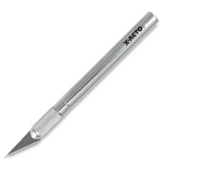
And for another dirty secret. When the spacing is unnecessary close defects will be more common. The type of defect to be expected for unnecessary small spacing is a short. Shorts can be reworked and this is typically done by using an X-Acto knife. If it makes you uncomfortable that a human hand and halo scope is being used to remove a short with a .076mm/.003” space, then please increase the space when it is possible. There will be less “Detected” shorts and less reworking with an X-Acto knife.
Best Practice Summary:
- If you contract your design to an outside service instruct them to maximize the spacing.
- Verify and document the design’s minimum conductor and space on the fabrication drawing.
- Specify the minimum allowed conductor and space. These values will be less than the designed minimum conductor and space widths.
- Maximize the conductor spacing to reduce waste, lower cost, improve fabrication yields, and increase reliability for the life of your product and program.
Special thanks to Michael Lowry for the reviewing this post.
More articles
From Layout to Fab: Gerry Partida’s Top DFM Guidelines for PCB Designers
Originally published July 10, 2025 by Judy Warner at The Electronics Eecosystem When it comes to ...

RF & Microwave PCB Design: Navigating High-Frequency Complexity with Precision
RF and microwave PCBs aren’t just signal carriers—they’re performance enablers. In the GHz realm, every ...

Understanding Controlled Impedance in High-Frequency PCB Design
Controlled impedance is crucial in printed circuit board (PCB) designs that operate at high frequencies ...