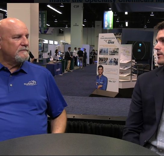
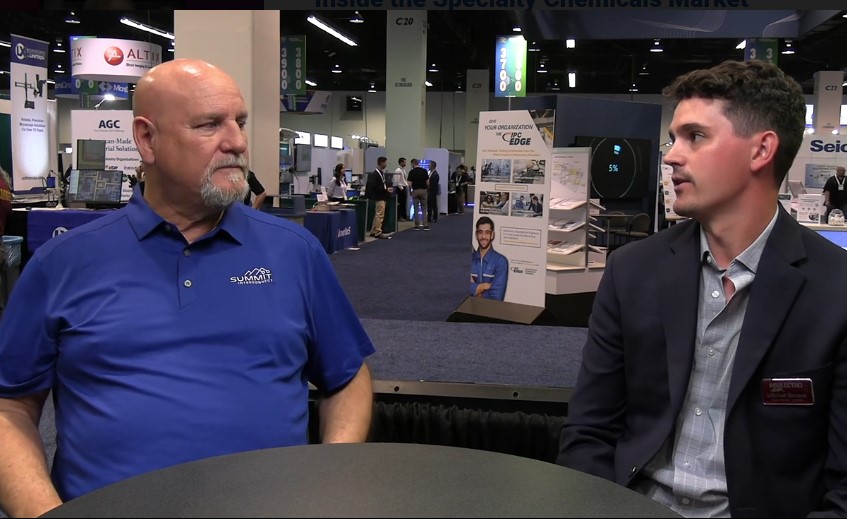
At the IPC APEX EXPO 2025, Mike Trammell of Summit Interconnect joined Mitchell Benson to discuss the future of PCB technology. Their conversation covered the latest advancements in PCB manufacturing, the push for miniaturization, and the increasing role of automation in the industry.
Breaking Micron Barriers with Advanced Materials
Summit Interconnect is leading the charge in high-density PCB manufacturing by pushing past traditional limitations.
Most manufacturers stop at 75-micron line and space dimensions, but Summit is currently operating at 40 microns and working towards achieving 30 microns. This miniaturization is critical for industries requiring ultra-high-density interconnects (HDI), including aerospace, defense, and next-gen consumer electronics.
To reach these new milestones, Summit is investing in advanced materials such as new dry films, high-performance laminates, and innovative substrates.
Next-Level Automation and Precision Engineering
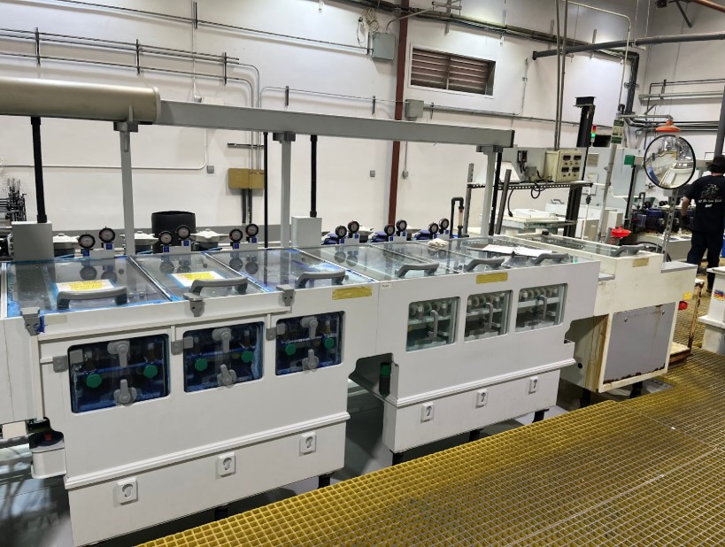
Summit’s commitment to automation is revolutionizing PCB manufacturing. The company has implemented advanced imaging systems capable of imaging down to 18 microns, with plans for further refinements.
Key investments include:
- Automated direct imaging systems for superior precision.
- Advanced etching systems across multiple facilities.
- Fully automated production lines integrating robotics, AI algorithms, and Industry 4.0 solutions.
Summit expects new automation to be operational within the next three months, demonstrating the rapid pace at which the company is embracing automation.
The Role of Young Engineers in the Industry’s Future
A crucial part of Summit’s success lies in attracting and developing young engineering talent. Trammell emphasized the importance of bringing in fresh minds, mentoring them, and integrating them into the company’s cutting-edge engineering culture.
Summit’s internal training program, combined with IPC’s educational initiatives, helps groom young professionals not just in engineering but in the company’s culture and innovation mindset.
A Call to Action for Future Engineers
The conversation concluded with a strong message for young professionals considering a career in the PCB industry.
Trammell reassured them: “You’ll never be out of work. You’ll never be bored. The days will go by fast.”
For those who love hands-on problem-solving and want to work with cutting-edge technology, the PCB industry offers limitless opportunities.
Summit Interconnect: Leading the Way
With continued investments in advanced materials, miniaturization, and full automation, Summit Interconnect is paving the way for the future of PCB manufacturing.
As the company pushes past current limitations, it’s clear that Summit’s innovations will continue shaping the industry for years to come.
More articles

What Companies Need to Know Before Entering the MilAero PCB Market
Beyond the Board: What Companies Need to Know Before Entering the MilAero PCB Market Originally published ...
Where PCBs Are Born: Touring a Quick-Turn Factory in North America
This article was originally published by Hardware FYI. ...

Orbital High Ground Why Space Superiority Is Slipping Away
“The next war might be won—or lost—22,000 miles above Earth.” That’s not science fiction. It’s the ...