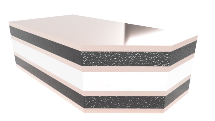
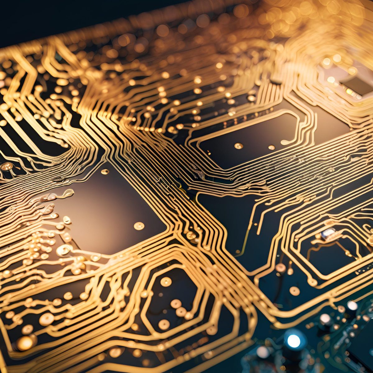
What is a Stackup?
PCBs are made of alternating layers of conductors and insulators (dielectrics).
Multi-layer PCBs are either made by laminating two or more premade cores together, or by starting with a core and laminating foil on the outside to build up the outer layers.
The conductor for rigid PCBs is almost always copper. Occasionally you will hear about aluminum in the middle of the board, but it usually is there to act as a thermal conductor, not an electrical conductor. The insulators are made of a variety of materials that range from inexpensive and easy to work with fiberglass to expensive and hard-to-fabricate Teflon (for RF designs.)
The copper layers are counted from the top to the bottom and referred to by their layer number: “Layer 1”, “Layer 2”, etc… Often, you’ll hear the layers referred to as other things, including “inner-layer”, “outer-layers”, “plane-layer”, “signal-layer”, “top-layer”, “bottom-layer”.
Symmetry
A general rule for designing a core stack is to ensure that it is symmetrical about the middle.
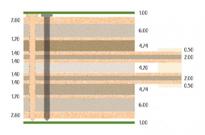
If your stack is not symmetric, differential coefficients of thermal expansion will likely cause the board to warp during assembly and operation. This is primarily a problem on very thin PCBs. Copper acts to constrain the expansion in places & directions where it is present but does very little to constrain expansion in lateral directions.
This type of warpage is caused by uneven copper etching on opposite sides of a core.
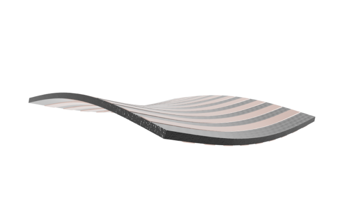
Most engineers know that they need to design a balanced layer stack to prevent warpage during assembly. But it's pretty often the case that engineers will remove large amounts of copper during the routing process resulting in an unbalanced stackup. If you don't keep track of your copper symmetry, you will end up designing a potato chip.
More articles
From Layout to Fab: Gerry Partida’s Top DFM Guidelines for PCB Designers
Originally published July 10, 2025 by Judy Warner at The Electronics Eecosystem When it comes to ...
Understanding Controlled Impedance in High-Frequency PCB Design
Controlled impedance is crucial in printed circuit board (PCB) designs that operate at high frequencies ...

Sustainability in PCB Design: Insights from Summit Interconnect at IPC APEX EXPO 2025
At IPC APEX EXPO 2025, Gerry Partida, VP of Technology at Summit Interconnect, sat down ...