When it comes to creating printed circuit boards, engineers often guestimate various aspects of their design. One such design metric is known colloquially as Trace and Space. Trace refers to the width of a particular copper track, and Space refers to the width of the gap between two adjacent pieces of copper.
The trace and space are based on a variety of factors. This post provides basic instructions on how to determine appropriate trace and space guidelines.
Impedance Control
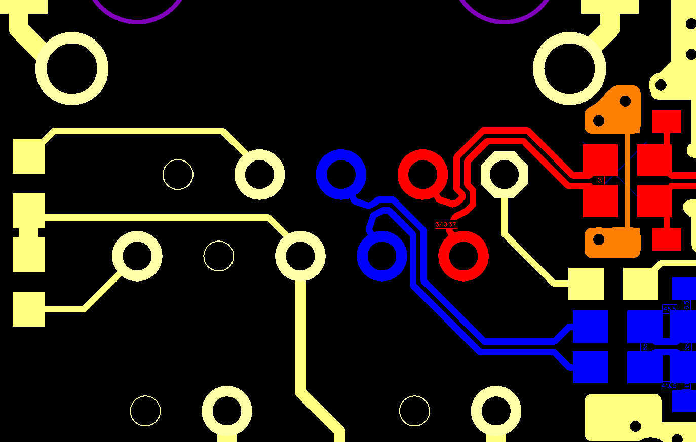
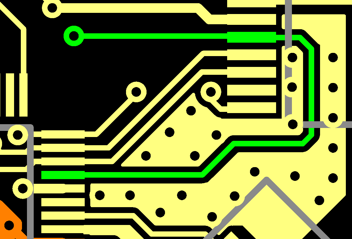
RF Engineers and High-Speed Digital Design engineers have to carefully route their traces (and their signal return paths) through the various layers of their boards. Dr. Eric Bogatin often states, “There are two types of Antenna Engineers: Those who know they are designing antennas, and those who don’t.” So, to keep the reflections and radiated emissions of your board low, you need a constant impedance on high-speed digital and rf nets.
Whenever a copper trace changes width, layer, or substrate, the speed of propagation changes and a portion of the signal is reflected or radiated into space. It is important that differential-pairs and single-ended high-speed digital signals are given route priority at the very beginning of your design to minimize layer transitions and traces from other nets should not cross above or below these lines unless there is a plane-layer between them.
Once you know you have an impedance-controlled trace on your design, you should communicate with your fabricator, who will determine the trace and space specifications you can use to route your design. The fabricators combine simulation software with real-world experience to determine the proper specifications.
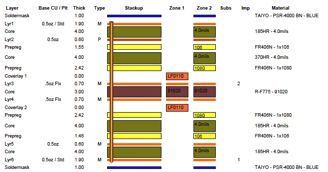
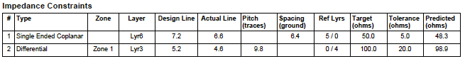
Each layer of your design has unique material properties and can potentially require different trace and space requirements to achieve a constant impedance. If you have a 7 mil-trace with 14-mil space on an external-layer, there is very little chance that those same numbers apply to the net when you transition to an internal layer.
Temperature Control
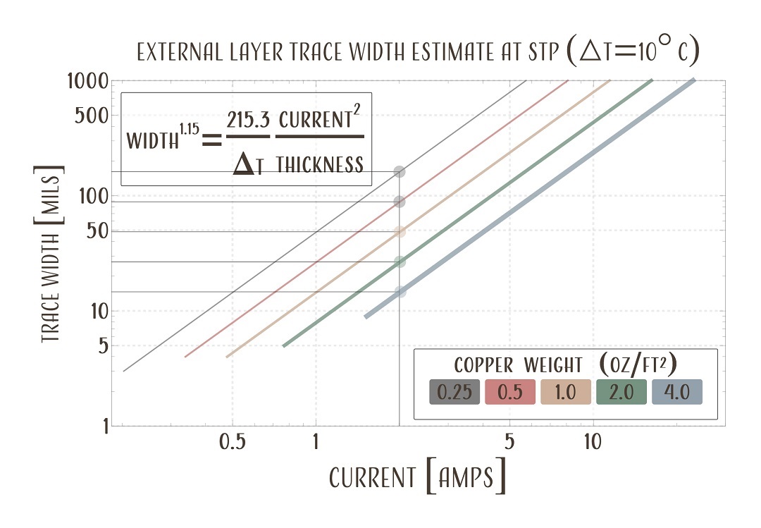
Power-design engineers are usually more concerned with their board bursting into flames than with their eye-diagrams closing. So, the question they usually ask is “How much current can I put through this trace?”. That answer was originally given in IPC-2221, which has been updated by IPC-2152.
IPC-2152 was released five years ago and should be used for estimates only. All prototypes should be field-tested before going into mass-production. Below is an updated graph to be used for estimates only.
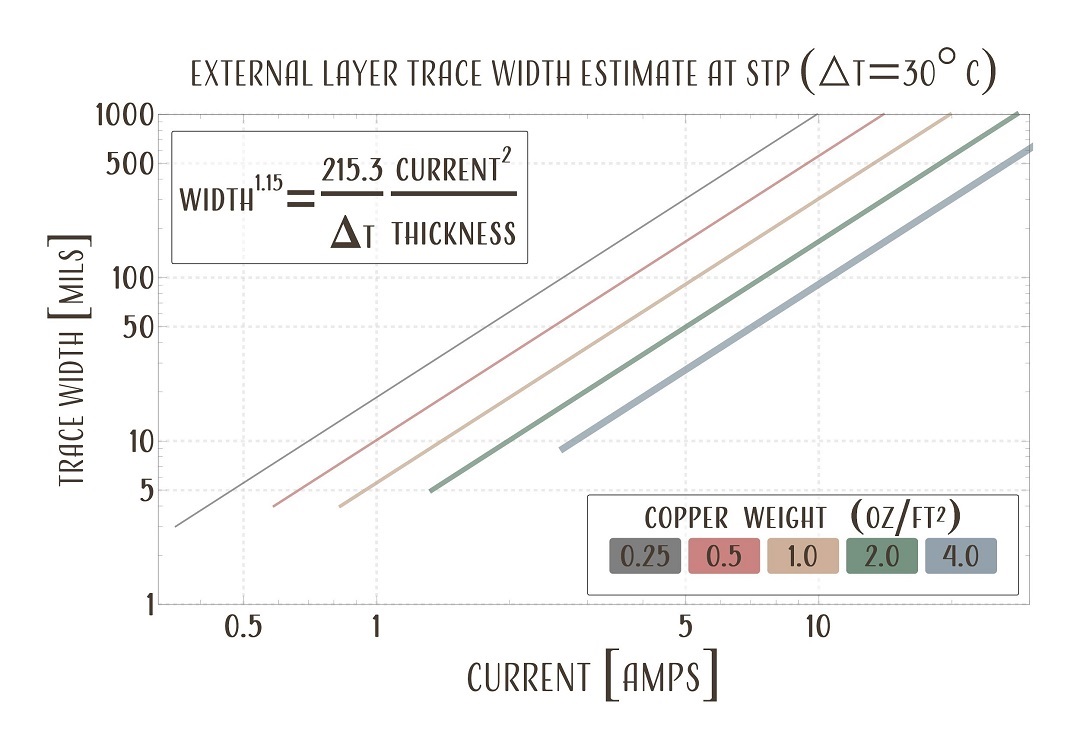
To use the graph package, determine the maximum safe operating temperature for your PCB substrate, as well as the maximum expected environmental conditions of the design as well as an appropriate derating factor. Maximums are not the only consideration. The stresses caused by mis-matched coefficients of thermal-expansion play a role as well. Thermal cycling at relatively low temperatures might destroy your design long before you ever approach an upper temperature limit.
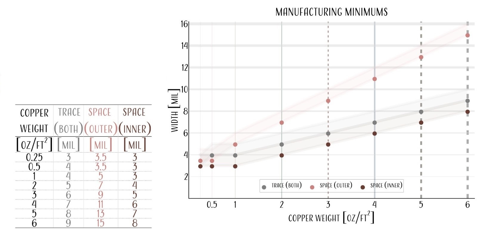
Manufacturing Minimums
Whenever a design pushes the absolute limits of manufacturing, not every board on a panel will work. The ratio of successes to tries is known as the “yield” and controlling the yield is critical to keep the cost of your design low. So, whenever you talk to a fabrication-house, and ask them what their absolute minimum trace/space guidelines are, you should also ask them what their “preferred” minimums are as well.
Conclusion
These are just three factors that affect your trace and space guidelines for ridgid circuit boards. Remember though, they are only guidelines. Engineers are ultimately responsible for the designs that they make. Make sure you give yourself time to test your device in the field.
More articles

Understanding Controlled Impedance in High-Frequency PCB Design
Controlled impedance is crucial in printed circuit board (PCB) designs that operate at high frequencies ...

Sustainability in PCB Design: Insights from Summit Interconnect at IPC APEX EXPO 2025
At IPC APEX EXPO 2025, Gerry Partida, VP of Technology at Summit Interconnect, sat down ...

The Key to First-pass Success in PCB Design
In the dynamic world of PCB manufacturing, achieving first-pass success hinges on more than just ...