
Every board designed is unique, has different requirements, and requires different trade-offs on the design, but there are basic guidelines of component placement that will go a long way toward creating a professional board that can be easily moved from the design table to reality.
Components
An overall strategy that will help considerably, no matter the soldering method, is grouping components into functional blocks. Not only does it help keep things organized and easier to track, but it also decreases the average track length and provides a good place from which to start. Once all of the parts have been grouped together, you can get an idea of about how much space you will need and can make a good approximation of the board size. Of course, the board size can change at any time, but it is helpful to have some loose constraints as it is natural to expand to fill the space provided.
Eliminate Shadowing with Proper Pad Placement
To avoid the shadowing effect, use a combination of staggering pads so that one pad is not directly behind another. Another option is to put enough space between the components so that the solder comes back together in time for the next part. Spacing between components needs to be a minimum of 25 mil but could be up to 100 mil if it is a larger pad. For reflow spacing, a general rule of thumb is that the parts can be approximately one half the distance required for wave soldering. In small infrared reflow ovens, where the board doesn’t move, if the infrared source of the reflow oven is not directly over a part, but at an angle, a taller part can leave the smaller part in a shadow. To avoid this effect, make certain the parts are not too close to each other if there’s a distinct height disparity. Please note: this issue is more prevalent with wave soldering techniques. When using other selective soldering methods, shadowing may not pose a manufacturing challenge.
Consider Component Size for Even Thermal Load
There are certain size restrictions that need to be considered for assembly. For example, if a main consideration for the design is size or if the board deals with high frequency signals, there may be the temptation, or even the requirement, to use passives in the 0201 or 01005 package sizes. However, if the board is going to be mixed technology and will be wave soldered, you should not use 0805 and smaller surface-mount devices because the surface area underneath the component is not sufficiently large for placing the glue properly. Beside size restrictions, care must be taken in terms of the thermal mass of adjoining components. If one portion of the board contains many large components while another portion contains only small passives, there will be a thermal mass imbalance across the board. For the solder and joints to reach the necessary temperature to ensure a good bond, the side of the board with a larger thermal mass requires a higher temperature than the side of the board with the smaller thermal mass. However, both sides are subjected to the same conditions. Either the larger components won’t be well soldered or the smaller components will be subjected to damaging levels of heat. By intermixing the two sizes as much as possible while still maintaining the functional blocks and avoiding shadowing, thermal load is spread more evenly across the board.
Align Polarized Components in the Same Direction
To reduce the opportunity for mistakes, it is also a good practice to align all polarized components in the same direction. All polarized capacitors, diodes, or LEDs should have their anode in one direction, cathode in the other. This information can even be silk screened or placed in the copper layer to help the assembler know how to place the parts. If a general direction is not provided, then properly labeling every polarized component is important for the same reasons. If the boards will be hand soldered, it will reduce the risk of human error on error on every board. Even for machine-populated boards, if the pick and-place is programmed incorrectly due to unclear polarization, it will be a very costly mistake.
Traces and Pads
The setup of the traces and pads can significantly affect the ease of assembly and rework required for your board. From skewed to tombstoned components, careful trace and pad design can practically eliminate these problems.
Avoid Tombstoning by Ensuring Consistent Thermal Loads
Tombstoning is a result of one side of a two-terminal device reflowing faster than the other. As the solder reflows and moves up to cover the terminal, it exerts force, pulling down and toward the pad. If that same force is not being exerted on the other side, as it has not reflowed yet, then the component will be pulled out of the solder paste on the other side and stand straight up, dipped in the reflowed solder. This vertical rectangle is reminiscent of a tombstone, which is why it is called tombstoning.
Control Solder Flow with Traces
Solder mask typically stops solder from flowing anywhere except on the pad. Without that protection, the solder can and will flow as far down a trace as possible. This flow down the trace is generally not a problem, however, the way it pulls components may skew them off the pad. If the forces on the component are not controlled, it can twist one end of the component so much that the other end comes off the other pad. This can be controlled with careful design. The simplest method is to have the traces leave the pad directly outward or inward. If this isn’t possible, then have the traces leave the pad in similar directions, which may pull the component in a certain direction, but should be straight and less likely to pull one end off a pad.
Create Thieving Pads to Reduce Bridging
For wave soldering surface-mount components, these two issues are not a concern as the components are glued to the board. The bigger concern for wave soldering besides shadowing is reducing bridging on high pin-count devices. This is done by creating thieving pads for your devices. As a long row of leads have the solder wave flow over them, the leads pull the wave from one lead to the next, depositing the correct amount of solder on each lead. However, at the end of the leads, the solder wave does not have any further leads to pull the wave along. The solder then creates a ball on the last lead, frequently creating a solder bridge between the last two leads. This is fixed by creating a larger pad on the trailing edge of the device. This larger pad has the surface area needed to wick the excess solder off the lead, pulling it away from other leads. It is important to ask your assembly partner what selective soldering processes are used in order to determine if thieving would be an issue or if design changes are necessary to ensure ease of automation.
The Board Itself
To ease assembly, the board itself needs to be taken into consideration. While boards can be made in practically any shape imaginable, odd shapes make automation very difficult.
Boards Should Have at Least Two Parallel Edges
To make sure that your boards can be gripped properly, you will need to provide at least two parallel edges. If the board needs to be circular, or some other odd shape, then the printed circuit board manufacturer can leave the boards connected to their larger panel while providing either V-grooves or rat bites so that the boards can be separated after assembly is complete. Do not forget to include overhanging parts, such as connectors, when deciding where the boards will be gripped. If there is an overhanging USB port or audio connector, it will interfere with the grip, and special grips will be required, adding another potentially expensive step to the assembly process.
Include Tooling Holes in Design
Tooling holes can be used throughout the manufacturing and assembly process. By providing tooling holes, boards can be stacked on top of each other, to reduce the amount of drills a machine must make. During assembly, these tooling holes can be used as mounting holes while in the pick-and-place for both placing components and applying solder paste. Tooling holes can even be used as fiducials.
Well-designed tooling holes can multitask to the point of assisting in electrical testing and in the mounting of a product’s enclosure. These tooling holes can be placed in the supportingportions of a panel or in each board individually. Tooling holes are standardized in size and it would be beneficial to speak to your board assembly house as well as the engineers designing the enclosure to ensure compatibility with all stages of the assembly.
Due to variances in the plating process, tooling holes are never plated. Minor variations in the size of the tooling holes could cause a myriad of issues, so in the read-me file you send your circuit board manufacturer, it is best to give explicit instructions to not plate certain holes.
Conclusion
The difference between an adequately designed board and a well designed board can be subtle yet substantial. While there is no strict method that will yield perfect results every time, knowing the tools at your disposal as well as the benefits and drawbacks of different methodologies will allow you to make well-informed decisions that will boost your yield, increase repeatability, decrease costs, and create an efficient design. With time, the tips and tricks introduced here will become a natural part of the process, and you will find particular methods suited to your design style, methods that will result in higher quality circuit boards.
More articles

6 Steps for an Accurate PCB Assembly Quote
Getting an accurate PCB assembly (PCBA) quote is essential to managing costs, timelines, and quality ...
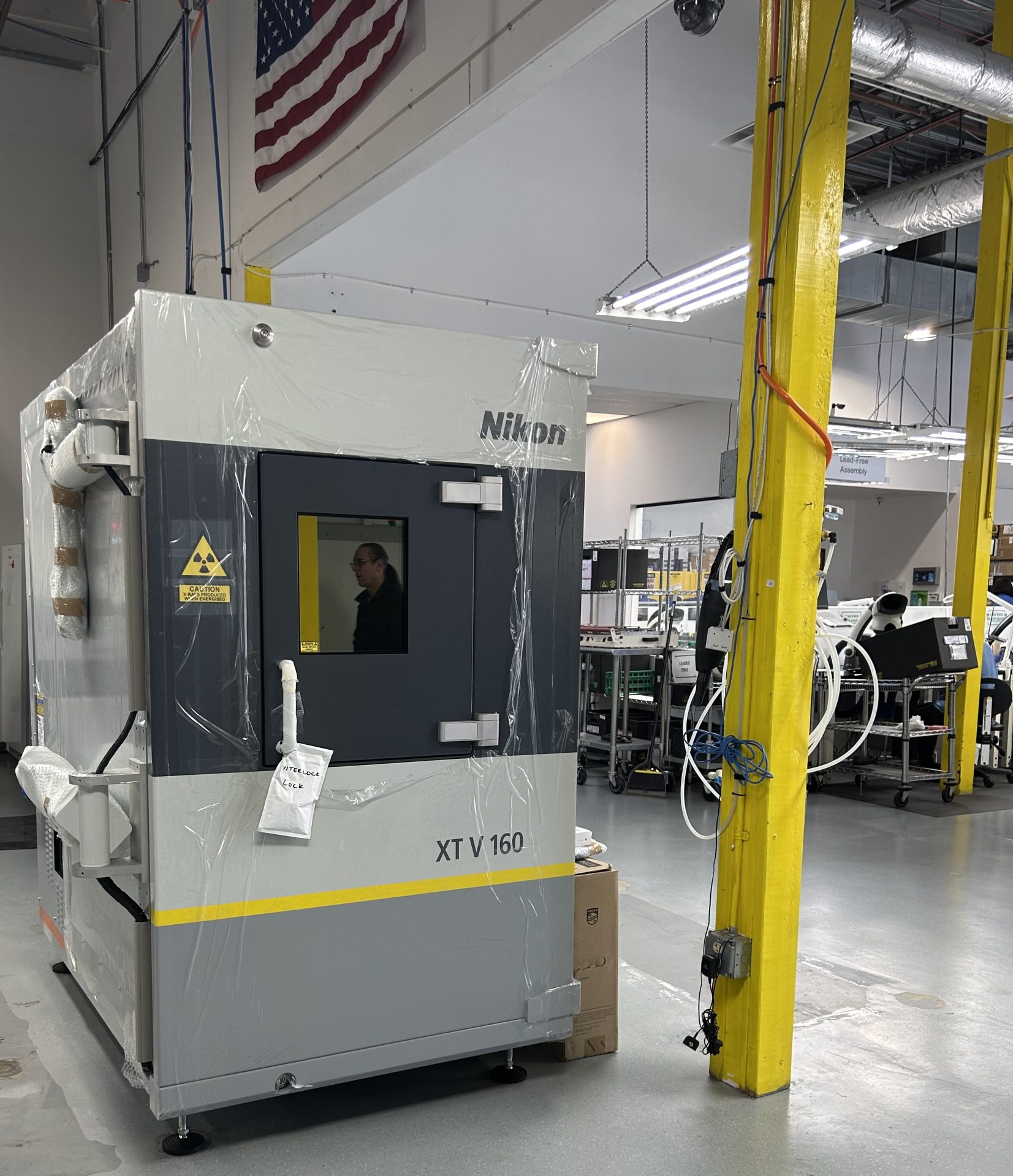
Summit Interconnect Enhances Assembly Capabilities with a Second Nikon XT V160 X-Ray System
Summit Interconnect is excited to announce the installation of a second Nikon XT V160 X-ray ...

Advanced Assembly Changes Name to Summit Interconnect
The Brand Transition Combines More Than 20 Years of PCB Assembly Experience with Extensive Fabrication ...