Build a better via stack by thinking about how your board is assembled.
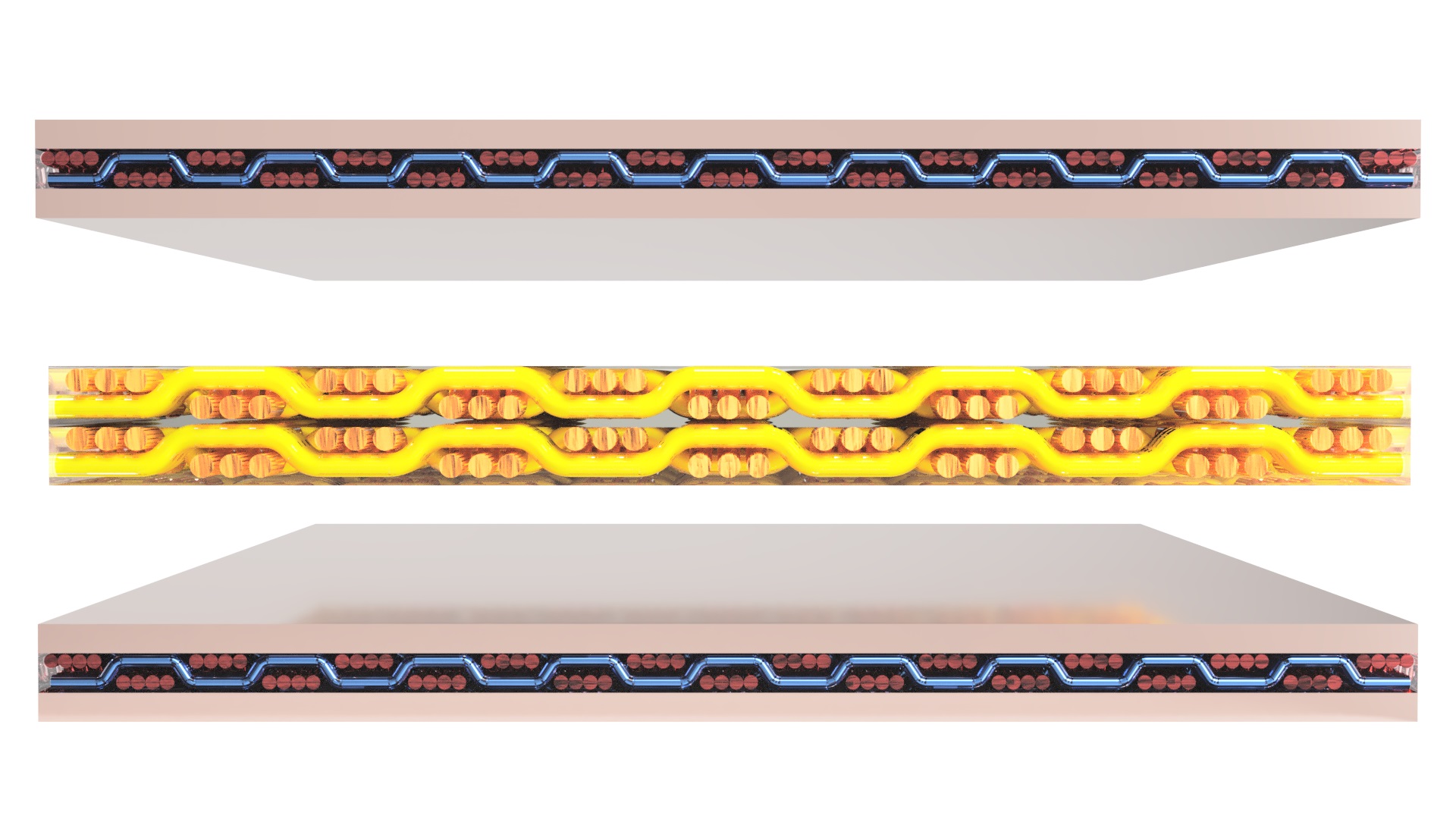
Cap vs. Foil Construction
Printed Wiring Boards are constructed in one of two ways described as “Cap” or “Foil” construction. The construction method determines via layer options and lamination cycles.
Foil Construction
In foil construction, fabricators start by drilling, electroplating, and etching a copper-clad core that will become the innermost layer of the design. Then additional layers of prepreg and copper are laminated to the outside of that core, and the new layers are drilled, electroplated, and etched. The process repeats until all layers of the board have been added, usually maxing out at 18-24 layers. After the last lamination, the board will be drilled, electroplated, and etched to create through-hole vias.
Very high layer count boards, such as a 96-layer board used for a new microcontroller validation, can be created by combining smaller layer stacks.
Microvias might be added to connect layers 1 and 2 or layers 3 and 4. To connect layers 1 and 3, a designer might create a through-hole via from layers 2 to 3 and then add a staggered microvia from layer 1 to 2. A through-hole via can be added after all layers are laminated.
Cap Construction
In Cap Construction, multiple copper-clad cores are drilled, electroplated, etched, and then laminated. If no blind or buried vias are needed to connect the cores, multiple cores can be joined in a single lamination cycle.
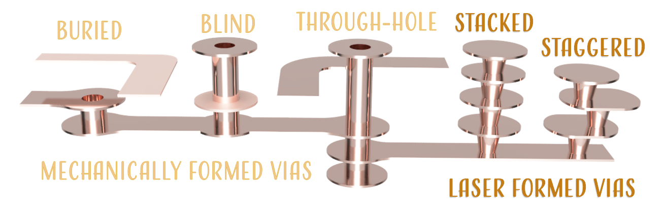
What does it take to make a via?
Mechanical Vias
After multiple layers of copper and dielectric material have been laminated in a hot-oil press, a high-precision drill pierces the complete-assembly or the sub-assembly in all the locations that will eventually become mechanical vias. Next, the panel is placed in a dry-film laminator and a negative-image of the layer artwork is projected on the film, curing it and causing it to adhere to the copper underneath. Then the uncured dry film is removed, leaving exposed copper in all areas that will eventually become traces, copper pours, and vias. The panel then enters an electroplating bath, where copper fills in the via barrels and thickens all exposed copper. Finally, the entire board is etched, which removes all of the unplated copper, and a small amount of the plated copper.
All mechanical (buried, blind, and through-hole) vias are formed in this manner. Buried and blind vias only take their names after additional lamination cycles.
Microvias
Microvias are usually created to join one layer to the next in a foil-construction. Under certain circumstances, a microvia can span two layers, but typically, the microvias would be built up one layer at a time in either a stacked or a staggered assembly.
Microvia holes are created with lasers that pierce through the topmost layer of copper and the underlying dielectric material. The combined thickness of the dielectric and copper is equal to the minimum allowable via diameter.
Microvias may be filled in a variety of ways, but electroplated copper is the most common option.
Why do you need to know all of this?
Once you know the basic processes required to make your board, you can determine whether or not the vias that you’ve specified can actually be formed in your PCB. Then you can start saving money in your next design by minimizing the number of lamination and via formation cycles.
More articles

Orbital High Ground—Why Space Superiority Is Slipping Away
“The next war might be won—or lost—22,000 miles above Earth.” That’s not science fiction. It’s the ...

RF & Microwave PCB Design: Navigating High-Frequency Complexity with Precision
RF and microwave PCBs aren’t just signal carriers—they’re performance enablers. In the GHz realm, every ...
How Embedded Heat Sinks Are Advancing PCB Fabrication
Managing localized thermal loads is increasingly critical as power densities rise. One solution to this ...