Your connection to advanced PCB manufacturing

Originally published in Design007, October 13, 2022
We recently spoke with Herb Snogren, an industry veteran and consultant with Summit Interconnect tasked with leading the company’s ultra HDI efforts. Herb is co-chair of the IPC ultra HDI subcommittee, IPC D-33-AP. In this interview, Herb discusses the current state of UHDI, how designers and fabricators can get started working in this new frontier, and why the U.S. must invest in UHDI technology now to counteract Asia’s near dominance of the UHDI segment, which has left some of our critical industries vulnerable to supply chain disruptions.
Andy Shaughnessy: Herb, almost everyone I talk to about this topic asks me, “What is the definition of ultra HDI?” What’s the manufacturable limit?
Herb Snogren: We’ve developed an IPC subcommittee, IPC D-33-AP. Jan Pedersen of NCAB Group is my co-chair, and we’ve defined ultra HDI as printed circuit boards that have line widths and spaces below 50 microns, and microvias at 75 microns and below in diameter. We came up with that delineation because of IPC-2226, which lists product attributes with producibility levels A, B, and C. Level C is the lowest producibility level and that stops at 50-micron lines and spaces.
Shaughnessy: Tell us about the committee’s efforts.
Snogren: What’s important to understand is that circuit boards are following the path of packaging substrates. We now have the term SLP (substrate-like PCB) because printed circuit boards, at least in Asia for small form-factor products, are being produced with manufacturing techniques similar to IC substrates. IC substrates now have line widths and spaces down to 6 and 8 microns, and that’s where we’re going. When you look at some of the Apple and Samsung products, they’re in the 20- to 25-micron line and space range in high volumes.
Shaughnessy: For years, we’ve been hearing that the convergence of IC and PCB processes was on the horizon. It seems like we’re finally there now.
Snogren: We are. Historically, IC substrates were made with semi-additive or modified semi-additive processing, and now printed circuit boards are being made with semi-additive and modified semi-additive processing. It is really happening.
Shaughnessy: Is Asia the center of ultra HDI?
Snogren: Yes. It really started with Apple working with their suppliers in Asia to get their line widths and spaces down. They did it in a big way, but because of that, other companies are taking advantage of the capability that’s been established. There are companies in other parts of the world that can do that. There may be one or two in Israel and Europe, but more than 95% of the volume is being done in Asia, with most of it in China.
Shaughnessy: What segments are driving the development of ultra HDI?
Snogren: It’s anything that has a small form factor. It started with the cellphone, just trying to pack more capability into a small space. You see it in medical devices that need to be small, such as in-ear devices or hearing aids. We need to do implantable devices that must be small and innocuous. With heterogeneous integration and cramming more transistors into a square inch through heterogeneous packaging, there are more I/Os on the device. The I/O density increases, so your pitch decreases, and that’s driving this as well.
Shaughnessy: Are design engineers from the PCB side studying IC laminate design processes, and vice versa?
Snogren: Product designers need to understand there is a manufacturing process capable of producing these finer features, and they can employ those in their products to reduce the size of the product or reduce layer count. The problem is you can’t get it in the United States, so if they design it, they don’t have a place to buy it here. You must go to Asia. Right now, companies are trying to develop it. Averatek has some licensees who can do this. Winonics (Additive Circuits Technologies) has a similar technology it is developing. But I don’t know if anyone is doing anything in a meaningful way or volume. Certainly not in any kind of volume at this point.
Shaughnessy: UDHI seems to be uncharted territory. What’s the biggest hurdle for fabricators who want to get involved? What will they need to learn and upgrade?
Snogren: On the equipment side, you must invest in direct imaging equipment that has 20-, 25-micron feature size capabilities or less. You find resists that are compatible with your imaging system. Then there’s AOI equipment. You need specialized plating equipment for doing simultaneous pattern plate and micro-via filling, and equipment for handling thin foil and ultra-thin foil, 1- to 3-micron foils, and differential etching equipment. If they want to go fully into semi-additive processing, they should look into something like Averatek or eSurface to get electroless copper to stick to a wide variety of laminates.
Shaughnessy: Because this is all build-up at this point, right? You can’t do subtractive at this level.
Snogren: It’s difficult. Asian fabricators were doing subtractive down to 30- to 40-micron lines and spaces. Once they hit that point, most of them started using modified semi-additive processes. One big aspect is cleanliness. I don’t know that any of us in the U.S. understand the cleanliness aspect of it, and how clean our processes must be. Once you start running in volume, those small particulates that don’t bother you when you’re at 3-mil line and space suddenly become a big percentage of a 20-micron line and space. We may have to deal with much different environmental issues in our factories with clean air, water, and processing tanks, ultra-filtration, special handling. It’s going to be different.
Nolan Johnson: It seems that we’re down to the dimensions that triggered cleanroom environments in the IC world 20 or 30 years ago, and that was very successful. We will be looking at that for our fabrication facilities in those dimensions as well, which will raise the cost of a UHDI facility.
Snogren: Yes, it will be difficult to justify having this cleanroom environment and ultra-filtered processes and air just to build standard 4-layer or 6-layer 4-mil line and space products. That’s why some Asian factories doing these types of products are specialized. All they do is build these HDI and ultra HDI products.
Shaughnessy: It seems like a big opportunity here for our fabricators.
Snogren: It’s a chicken or the egg scenario. You must develop the capability and hope people will buy it. But if you don’t develop the capability, they won’t even design those features because they can’t get it. It’s a tough investment decision to make for companies in North America. But I believe if you have the capability and demonstrate it, people will begin to design products that take advantage of that capability.
Shaughnessy: Will UHDI change the PCB designer’s job?
Snogren: The HDI design standards in IPC-2226 don’t really address some of the requirements for feature sizes, alignments, and spaces below 50 microns very well. That’s something that our D-33-AP committee is trying to address. How do the design standards need to change or how do we need to adapt them for ultra HDI features? Here are some things that we’ve already identified: The plating thickness requirements, annular rings, and dielectric thicknesses are different. We may not even use foil in some of the semi-additive applications, and many of the design standards don’t address that. Of course, 6012 needs to be modified as well to allow for thinner copper conductors because they’re not doing 1 mil or 1.2 mils of plating on line widths that are 20 microns and below. They’re typically in the 12- to 18-micron thickness range, which doesn’t meet 6012. Solder mask thicknesses may need to decrease when you have devices with 0.2-millimeter BGA pitches; you can’t have thick solder mask or you get a standoff.
Shaughnessy: What about EDA tools? Can they go down to the 20-micron level?
Snogren: Yes. That’s not a problem as far as EDA tools go, because a 25-micron line is just another D-code in the system. Some of the design rule criteria would be different, certainly, such as the annular rings. Some of the requirements that you would have on the drawing with conductor thickness or plating thicknesses would be different.
Shaughnessy: It seems like, as far as signal integrity, there would be a lot of advantages, but still quite a few hurdles as well.
Snogren: Yes. UHDI can be beneficial in one way: You can certainly get a higher precision line width and spacing when you’re doing semi-additive processes because your etch loss is virtually nothing. You can be very precise, but you’re dealing with very small features and any minor imperfection will cause an issue that you wouldn’t see on a 3-mil line and space job.
Shaughnessy: It seems like at this level you would want to simulate and run analysis every time?
Snogren: Yes, and you need to do that in conjunction with the fabricator because there are so many different techniques now for manufacturing a given feature. You can do it with subtractive, semi-additive, or modified semi-additive. They will all give you a slightly different result in maybe conductor thickness or tolerance. You must work in conjunction with the fabricator, understand their process, what the result will be, and design around their process. It’s no longer just designing it, throwing it over the fence, then seeing who will snap it and try to build it. There must be more cooperation between the designer and the fabricator.
Shaughnessy: I mean, you’re not going to start off an ultra HDI project without already having your fabricator selected. You’ve said that some vias are the thickness of a human hair?
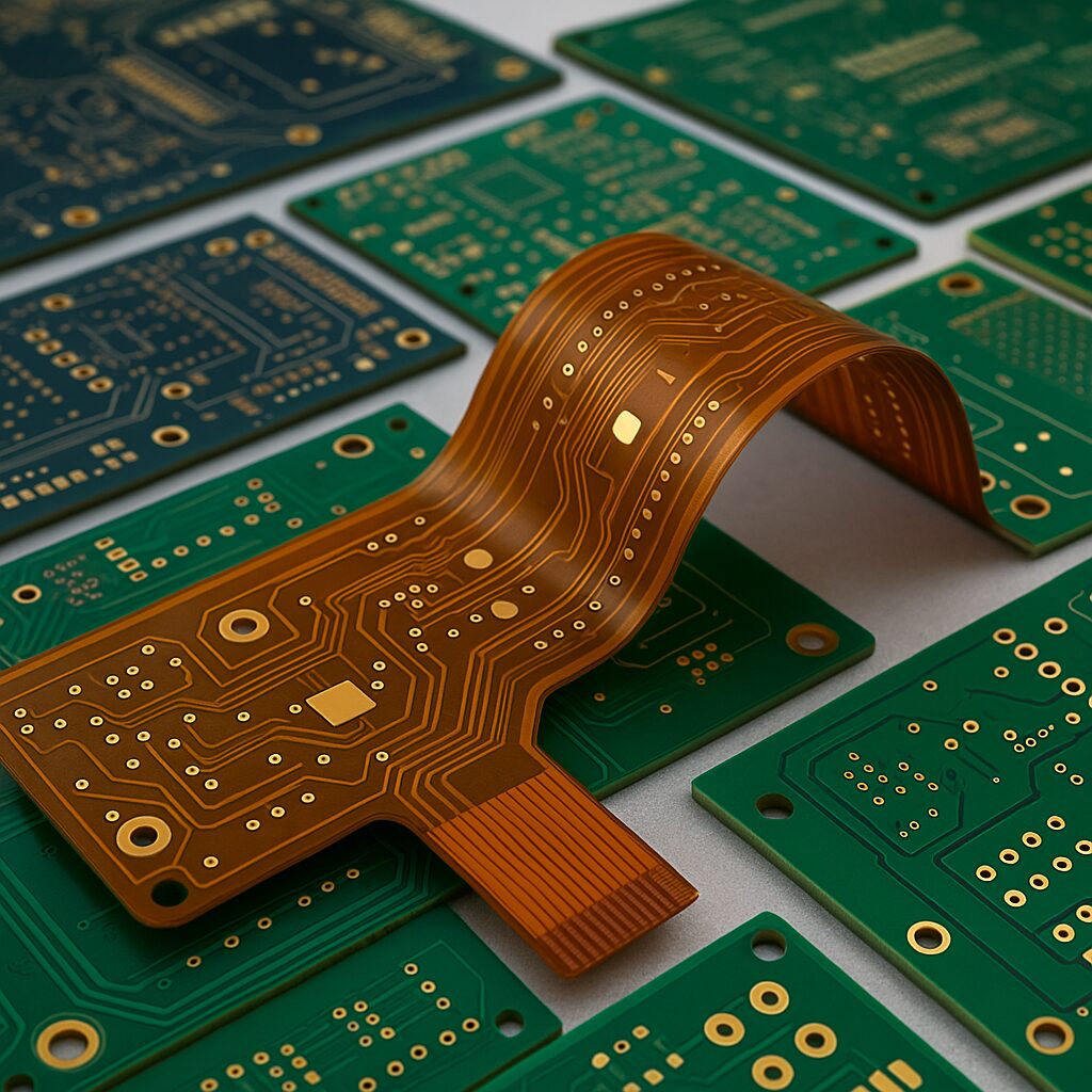
Snogren: That’s right. They’re getting down below 3 mils in diameter. You’re looking at 25- to 50-micron diameter microvias.
Shaughnessy: That’s really intriguing. What does the typical UHDI process look like?
Snogren: It will be a buildup technology, where you start with a core and sequentially build layers on both sides as you go, using microvias as an interconnect between the layers. In some ways that’s easy because registration is so simple. Each layer automatically registers to the layer below it, and you really don’t have the kind of misregistration that we have with regular multilayer boards and blind and buried vias. It’s a sequential process. If you have five lam cycles sequentially, and you screw up the last one, you just burned up two to four weeks of work and you have to start over.
Shaughnessy: Now, much of this wouldn’t have been possible even 10 to 15 years ago because these enabling technologies didn’t exist, right?
Snogren: Direct imaging is a big one. That has helped with registration and feature size capabilities. When we were using film in the past, we had registration issues because the film moved, and we had to register it manually. It expanded and contracted with temperature and humidity. We had to pin it and the pinning wasn’t always perfect.
Now we can have much smaller annular rings, much smaller feature sizes. With film, typically we had a really hard time getting down to 2-mil lines and spaces consistently when we were using a phototool. Not that it can’t be done because they use phototools for ICs, but they’re tiny and they use stepper cameras. They’re not doing panels on a single sheet of film. Direct imaging is probably the biggest example. Anybody can buy a direct imaging system that can go down to 12 microns and maybe even less if you want to spend the money. If you get the right resist, you can resolve 20-micron lines and spaces fairly easily. That was unheard of 10 years ago. You couldn’t even think about it.
Shaughnessy: Where are the bottlenecks in this whole process? Where do we need to innovate?
Snogren: It’s just adopting the thin foils. Designers need to understand what the manufacturing process is like so they can design around it, whether it be using thin foils or semi-additive process with electroless copper. It’s about understanding what the copper thicknesses will be, what the feature size capabilities are. For the fabricator, it’s about getting the systems in place: the direct imaging system, AOI, electrical test, differential etch, the proper via fill and laser drill capabilities. HDI manufacturers already have these, so it’s just a matter of adapting them to a slightly different process flow and adding a few other processes.
Shaughnessy: I keep hearing about the Asian companies doing UHDI well and for fairly cheap. What do we need to learn from them?
Snogren: They’ve already adopted modified semi-additive processing and semi-additive processing. With the modified semi-additive processing, which gets you down to 20- or 25-micron lines and spaces relatively comfortably, we must copy what they’re doing. Remember, when they do this in Asia, it’s in a factory that was designed to do nothing but that. They’re not building a wide variety of products; they’re only doing ultra HDI.
Shaughnessy: Those are all greenfield facilities.
Snogren: It’s what they do all day, so it’s a fairly standardized well-controlled process where they build things that are within a narrow design feature range.
Shaughnessy: What percentage of ultra HDI now is mSAP or A-SAP?
Snogren: When you look at printed circuit boards on the high-end cellphones, watches, and things like that, almost all of that is mSAP. The semi-additive process really is being used more on the packaging substrates, and they’re using either electroless copper or vacuum-deposited copper on those products. I don’t know that many circuit board manufacturers are trying to use semi-additive processing in volume anyway. But with Averatek, the licensed companies are starting to use that. It’s certainly a viable way to approach it.
Shaughnessy: You mentioned that our process, our technologies, should learn to be more like the semiconductor industry, that we should learn from them. What are some things that we should take away from the way semiconductor manufacturers have been doing it?
Snogren: When they design a factory, it’s around a capability. They deal with a process node and technology node, and if you’re a semiconductor designer, you design into that node, you design into that factory. They don’t just accept any design. They give you the design criteria in a file and you must follow that criterion. If you don’t, they don’t build it.
Shaughnessy: We had a magazine focused on design rules several months ago. With ultra HDI, will we need to have some uniform design rules and constraints?
Snogren: We need some general ones, and my IPC committee is working to develop those guidelines. We are developing a general guidebook for UHDI. We don’t want it to be locked into any one process, because many diverge from IPC-222x and IPC 60xx standards. We’re trying to make it process agnostic as much as possible. We want it to be more general, suggesting that the designers talk to and work with their suppliers more closely on the design because they may use multiple techniques to fabricate the job. We haven’t even talked about fully additive with inkjet printing conductors.
Johnson: When we start talking about UHDI, do you see that as the tipping point where cleanroom technology needs to happen? Is UHDI where we move to just greenfield facilities?
Snogren: For volume, yes. If you want to do volume and repetition, and do things with good yields, there’s no doubt in my mind that’s the case. For small companies in the U.S. that want to offer that as a capability, I don’t really know where we start to run into the hurdles. I’ve been running some testing on 25-micron lines and spaces here and I haven’t gotten to the point where it’s become an issue, but we haven’t really done a lot of volume. A dedicated facility is the way I would go for high volume. For an existing HDI factory, I believe one can produce small quantities of UHDI product with a decent cleanroom for the imaging processes and good filtration in electroless copper and electrolytic copper plating.
Johnson: Now it starts to feel like integrated circuits where, as you were saying, you build the factory around a particular technology. It feels like we’re on the cusp here of having the cutting-edge printed circuit board fabrication philosophy start to look like IC.
Snogren: Yes. And when Apple decided it needed UHDI, the company didn’t just throw designs over the fence and get somebody to build it. They went to companies like AT&S and Multek, and said, “Here’s where we need to go. Here’s our roadmap. Start developing capabilities to get there.” They started doing that in factories that were already pretty specific to a certain application, like IC packaging. I have friends who worked at a Multek HDI factory in Zhuhai. They said Apple and Samsung were migrating from 50-micron line and space to 40 and 35, then saying, “We’ve hit the wall in this factory. We’re having to build a factory somewhere else that’s going to do mSAP.”
Johnson: Well, that’s a fundamental shift for thinking in North America, for sure, and Europe as well.
Snogren: You can’t be all things to all people. That’s the thing. Multek is a good example. On their campus in Zhuhai, they have an HDI factory, a flex factory, a daughter board factory, and a back panel factory, and they’re very segregated for a very specific type of printed circuit board.
Shaughnessy: Are there any good resources to learn more about ultra HDI, maybe in the form of websites, books, or instructors?
Snogren: Yes, there are a few resources, but not many. I learned about semi-additive processing when I first started.
Shaughnessy: How did you get into ultra HDI? Your father, Richard, wrote for me years ago.
Snogren: My father owned a circuit board factory, Reliable Circuits in Clearwater, Florida, when I was in high school. I worked there during college. After college, I worked at a couple of circuit board shops in Denver. Then my dad and I decided to start a shop in Colorado back in the mid-’80s, and we ran that for 16 years. I went to Coretec for a while, and then got hired as a consultant by Viasystems. I was in China for four years at the Guangzhou factory and the Zhongshan factory. I got to see another side of things. It’s just ridiculously high volume.
I’ve been working with smaller companies recently, like Royal Circuits, which was acquired by Summit. I helped Royal Circuits develop its HDI capability several years ago. But the migration into ultra HDI really came through my work with the DoD and the PCB executive agent. I’m on the IPC-1791 committee, and we were talking about whether we should include IC substrates into IPC-1791. We found out there really aren’t any industry design or quality standards for substrates. I started researching it a little bit and educated myself about IC packaging. I realized that not much happens in the U.S., certainly none of the fabrication of the substrates. This led to the creation of the IPC-D -33-AP committee to develop design and product performance standards for UHDI PCBs.
Shaughnessy: What does your roadmap look like for UHDI?
Snogren: We developed a roadmap at Summit. I said, “Look, you’re proficient now at HDI. You can do an eight- and 10-layer buildup board with five lam cycles and stacked microvias. You’re good at it, but you are limited to 3-mil line and space. Let’s put a roadmap together to get down to a 25-micron line and space because, if we can develop that capability, I believe we can get designers to design around that. We’re not going to have a lot of competition.” We put together a roadmap that we’re in the process of implementing. We’re not there yet, and we’ve got a couple pieces of equipment we need to buy, but we’re moving in that direction and it’s feasible.
Shaughnessy: This is the roadmap that you show your customers or is this internal?
Snogren: It’s internal now. We have established the direct imaging equipment capability and the dry film capability. We have the inspection and test equipment capability. We need to upgrade our microvia filling system and purchase a differential etcher. Once we have the via filling system and the etcher, we’ll be able to produce products with 25-micron lines and spaces. Whether our yields are going to be great, I don’t know. But typically, these are tiny little boards so even if the defect density is a bit high, we will still have good board yields within a panel.
Johnson: Right. What do we tell designers?
Snogren: First, work with a vendor or several vendors to determine whether they can lay out a manufacturing roadmap. The roadmap for many OEMs could say, “We’re seeing finer-pitch BGAs. We’re going to have to use 0.3-mm or 0.25-mm BGAs and we’re going to need 25- and 30-micron lines and spaces. We need you all to get there because we have a whole line of products coming in the next few years that require this.” Then you pick a process and say, “We’re going to use ultra-thin foil. I can already buy 1.5-micron foil, so we’ll start developing this capability slowly and put together the roadmap.” The designer can work with the fabricator to establish the design criteria and test vehicles and put that together. The fabricator will need to buy some equipment to support that.
From a designer standpoint, if they don’t want to go straight to Asia and get what they want, they need to work with a fabricator and design around the fabricator’s capability or develop that capability along with the fabricator. But it’s the chicken or the egg. As a fabricator, do you invest in that capability? It’s going to cost you money if you don’t have potential orders coming in.
Six to eight years ago when you bought an LDI machine, you were limited at maybe 2-mil lines and spaces. Then they went down to 1-mil line and space, but they were expensive. Now, if you’re buying a new direct imaging system, there’s no reason not to get it with 25- or 12-micron line and space capability.
You can buy an LDI machine today for not a lot more money that’s capable of getting you into ultra HDI, while it’s still going to support doing your 3- to 4-mil line and space jobs. That’s what happened at Royal Circuits. We bought a machine, not even for that capability, and I found out, “Hey, I can do 25-micron line and spaces on this thing.” We didn’t even plan for that one.
Shaughnessy: Herb, thank you for your time today. This has been very informative.
Snogren: Happy to help. Thank you, sure.