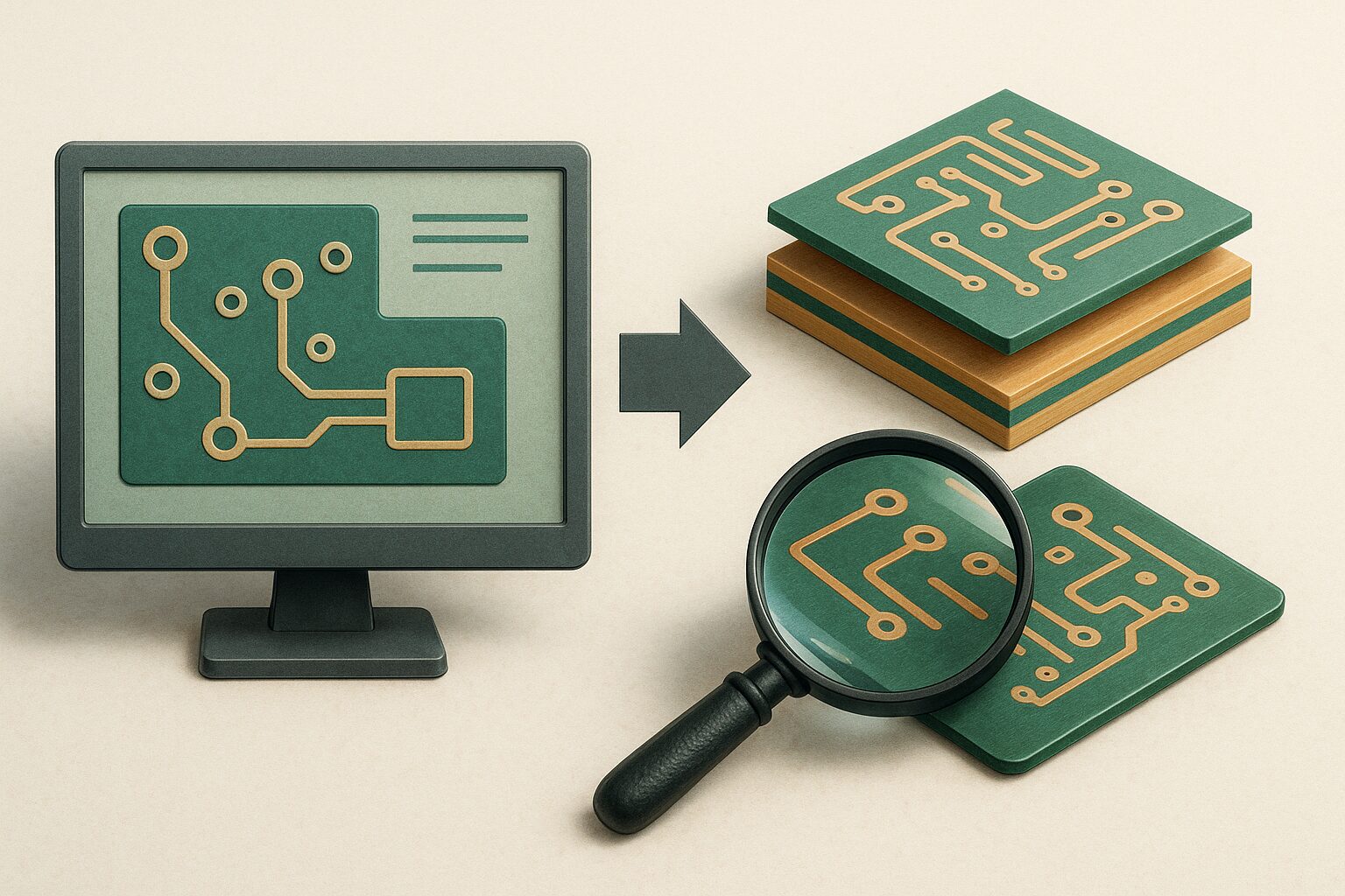
Your connection to advanced PCB manufacturing
Component selection and placement decisions go hand in hand and when one is misjudged, the entire design can suffer. With today’s increasingly dense and complex PCB layouts, even experienced engineers can overlook critical design details that affect functionality, manufacturability, or mechanical fit. These issues often surface late in the development cycle, leading to delays, rework, or costly design revisions.
To help avoid those setbacks, we’ve outlined seven commonly missed elements in component selection and placement. Whether you’re designing your first board or refining your process, these reminders can help ensure your layout is robust, efficient, and production-ready.
- Not making sure components fit inside the packaging after the PCB is assembled
Becoming too fixated on selecting working components but ignoring how they fit inside the packaging will result in a nonfunctioning or compromised design. When this happens, the chassis must be redesigned altogether, which could compromise the original vision and require starting the component selection process over from scratch. This headache can be avoided altogether if the components’ height clearance is observed from the start. Since height clearance restrictions vary by component, it is best to draw a basic board shape outline during the early stages of design, taking care to place some of the larger components where they may go on the board. This allows for quick visualization of the components’ position relative to their heights. - Neglecting to consider the pros and cons of SMT and FTH components for each circumstance
Surface-mount-technology (SMT) components are, on average, less expensive and more readily available than fixed-through-hole (FTH) components, but this does automatically qualify them as a better choice. Part density, power dissipation, size of the PCB and how the soldering pads will be accessed for debugging are all factors to consider early in the design stage. SMT components may be preferred for smaller PCBs, but soldering them by hand is infinitely more difficult without a reflow oven. In contrast, through-hole components can be adequately soldered by hand if the PCB is large enough. - Not having enough bypass capacitors and ground planes
Designers should ensure that a sufficient amount of bypass capacitors and ground planes are used in the PCB. Failing to place bypass capacitors across from the power and ground pins on the appropriate IC pin results in a circuit with nonoptimized electromagnetic compliance and compromised performance. Similarly, the correct number of decoupling capacitors must be placed near the supply to a ground plane, or some other ground location, when using integrated circuits. - Not checking for virtual part footprints
Rather than solely reflecting the number of components and raw materials needed to manufacture an end product, the bill of materials (BOM ) can also be used to reveal the number of virtual parts, which do have footprints associated with them and are not transferred to the layout. Virtual parts are used for simulation and need to be replaced with parts that have actual footprints, so do not forget to include them in the BOM. - Not thoroughly reviewing the BOM
Forgetting to thoroughly review the BOM report may leave part, vendor, and manufacturer information incomplete and disorganized, thus creating an inaccurate representation of the total cost. The BOM will not fulfill its purpose without complete information. - Not using reference designators
Failing to closely number reference designators will overly complicate the reviewing process of the BOM and prevent accurate sorting. - Forgetting to verify spare gates
In the haste to assemble a prototype, it can be easy to forget to verify that all spare gates’ inputs are connected to a signal. If spare gates are not connected to a signal, there is nothing in place to prevent the inputs from floating, thereby running the risk of compromising the entire system and preventing it from properly functioning. Debugging is a headache that can otherwise be avoided with thorough inspection. Therefore, it’s important to review all forgotten or spare gates to ensure that the inputs are connected.
Conclusion: Design Success Starts with the Right Details
Every PCB project hinges on careful planning and attention to detail—and component selection and placement are among the most critical early decisions. Overlooking even a single factor, like packaging constraints or missing bypass capacitors, can cause issues that ripple through prototyping, manufacturing, and even field performance.
By proactively checking these commonly missed elements, engineers can streamline their design process, reduce production delays, and deliver boards that meet both functional and mechanical requirements. Investing time upfront pays dividends later—and helps ensure your next PCB build moves from concept to completion without unnecessary setbacks.