Your connection to advanced PCB manufacturing
Originally published July 10, 2025 by Judy Warner at The Electronics Eecosystem
When it comes to practical, actionable DFM (Design for Manufacturability), I have one go-to person: Gerry Partida, VP of Technology at Summit Interconnect.
I’ve known Gerry for over a decade and have always appreciated how he brings clarity to the often-murky space between PCB layout and fabrication. With more than 25 years of experience preparing fabrication files, Gerry has become a trusted authority on all things DFM.
Early in my career, I spent 16 years selling PCB fabrication services. I worked closely with designers, engineering teams, and manufacturing managers–constantly bridging the gap between design engineers and front-end engineering teams at board shops. Over time, it became crystal clear that a successful PCB design didn’t just rely on the designer, but equally on the skill, DFM expertise, and communication of the fabricator’s front-end engineer. That perspective sharpened my ability to recognize real DFM talent—and Gerry stood out from the start. He’s been my go-to expert ever since.
So today, I’d like to (re)introduce you to Gerry and pass along the top DFM lessons I’ve learned from his decades of experience. I hope these insights help your next design handoff go more smoothly—and help you avoid costly delays or respins.
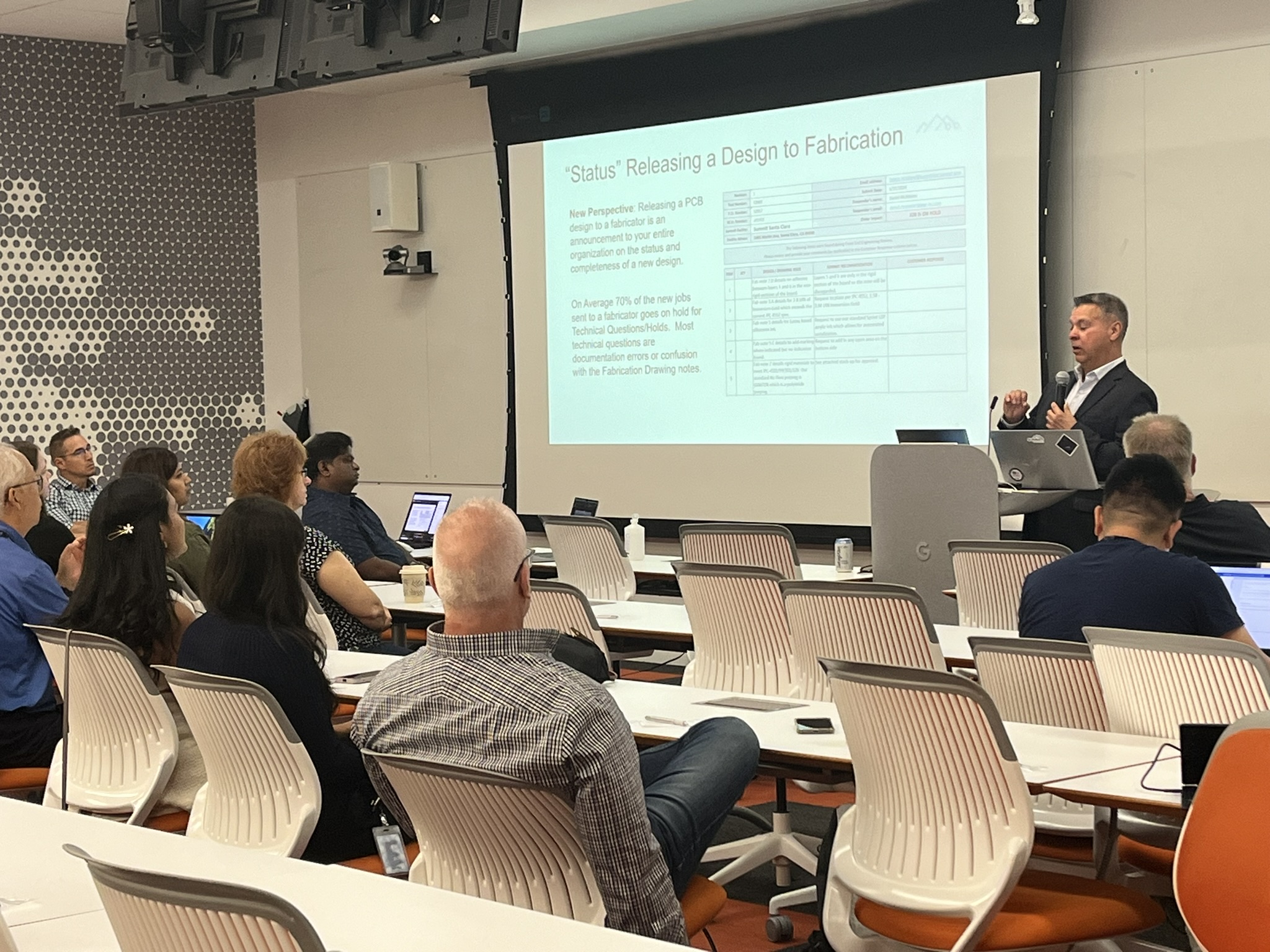
Top Seven DFM Tips I’ve Learned from Gerry
Here’s a concise list of DFM best practices Gerry consistently emphasizes:
1. “Control what you can control.”
This is Gerry’s cornerstone principle. Don’t leave critical manufacturing decisions—like stackup, padstack specs, or impedance targets—to the fabricator. The clearer and more intentional you are, the better your outcomes.
2. Don’t assume your fabricator knows your intent.
Designers often assume their fab house will “get what I mean.” They won’t. Be explicit—especially around impedance control, materials, and via structures. When possible, include supporting data.
3. Communicate early and often.
Working on a high-speed or complex board? Reach out to your fabricator before finalizing your design. A 15-minute call could save you days—or even weeks—of production delays.
4. Avoid Gerber-only packages.
Gerbers alone are risky. Provide a full data package with intelligent formats like ODB++ or IPC-2581, plus fab drawings, netlists, and material specs to avoid misinterpretation.
5. Don’t recycle old fab notes.
Copying fab notes from previous designs without reviewing them is a common mistake. Always update notes to reflect the current design and manufacturing requirements.
6. Be realistic with annular ring and drill tolerances.
Just because it passes in CAD doesn’t mean it will work in the shop. Account for drill wander and registration tolerances when defining via and pad sizes.
7. Know your fabricator’s capabilities.
Not all shops are built for HDI, flex, or RF boards. Match your design to your fabricator’s strengths—and if you’re unsure, ask early.
Why This Matters
As Gerry often says: “A design isn’t successful until it’s built, tested, and shipped—without drama.” And that success starts long before your board hits the fab floor.
Too often, designs are delayed or rejected because critical data was missing, assumptions were made, or documentation was unclear. The fix? Start thinking like a manufacturing partner, not just a designer.
If you’re a layout engineer, hardware designer, or someone who regularly interfaces with your CM or fabricator, you owe it to yourself to learn from experts like Gerry Partida. His practical wisdom has saved more than a few projects and reputations.